Semiconductor Silicon Wafer Market Size Analysis:
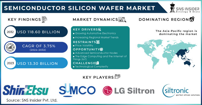
The Semiconductor Silicon Wafer Market was valued at USD 14.16 billion in 2023 and is expected to reach USD 22.61 billion by 2032, growing at a CAGR of 5.37% over the forecast period 2024-2032.
An increase in the efficiency of wafer fabrication and advances in 300mm and 450mm wafer fabrication techniques are driving the growth of the semiconductor silicon wafer market across the globe. Supply chain and sustainability initiatives aim to minimize waste of materials, increase energy efficiency, and enhance firm access to a stable supply of raw materials. Information containing Wafer performance and process metrics, e.g. defect density, resistivity uniformity, and flatness all contribute to improving chip performance. High-Purity Silicon Wafers Propelled by Growing Demand Across Applications such as AI, 5G, EVs, and Consumer Electronics, Innovations in SOI and SiC Wafers Enables Next-Gen Semiconductor Development.
Semiconductor Silicon Wafer Market Size and Forecast
-
Market Size in 2023: USD 14.16 Billion
-
Market Size by 2032: USD 22.61 Billion
-
CAGR: 5.37% from 2024 to 2032
-
Base Year: 2023
-
Forecast Period: 2024–2032
Get E-PDF Sample Report on Semiconductor Silicon Wafer Market - Request Sample Report
Semiconductor Silicon Wafer Market Trends:
-
Rising semiconductor demand across AI, automotive, and consumer electronics is driving wafer consumption, with global silicon wafer shipments exceeding 14 billion square inches annually, growing at 6–8% CAGR.
-
Expansion of 300 mm wafer production is strengthening market share, accounting for over 70% of total wafer revenue due to higher efficiency and lower cost per chip.
-
Increasing adoption of advanced nodes (≤7 nm) is boosting demand for ultra-flat, high-purity wafers, improving device density by 30–40% per generation.
-
Growth in automotive and power electronics is accelerating uptake of specialty wafers, with the automotive semiconductor segment expanding at over 10% CAGR.
-
Investments in new fabs across Asia-Pacific and North America are increasing wafer capacity, with over USD 100 billion allocated globally for semiconductor manufacturing expansion.
Semiconductor Silicon Wafer Market Key Drivers:
-
Rising Demand for Semiconductor Silicon Wafers Driven by EVs Consumer Electronics 5G AI and IoT Expansion
The rising consumption of consumer electronics, electric cars (EVs), and renewable energy applications is mainly driving the semiconductor silicon wafer market. In addition, the rapid surge of 5G technology, AI, and IoT devices has further increased the adoption of better semiconductor components and consequently drives the demand for silicon wafers. A principal driver has also been the increasing use of EVs and automated driving technologies, which has driven the power semiconductor market significantly to the automotive segment. The growth of data centers and cloud computing infrastructure is also adding to the growth since high-performance integrated circuits need to be made on silicon wafers. Meanwhile, new government measures to bolster domestic semiconductor manufacturing as well as investment in chip manufacturing plants are improving the stability and resilience of market supply chains.
Semiconductor Silicon Wafer Market Restrain:
-
Manufacturing Complexity and High Costs Restrain Semiconductor Silicon Wafer Market Amid Advanced Node Challenges
The Complexity of Manufacturing Processes among Major Restraints in Semiconductors Silicon Wafer Market When it comes to advanced semiconductor nodes, like the new 5nm and below levels, controlling wafer purity, defects, and high yield rates becomes much more challenging. Production of higher-performance chips requires more exacting fabricating technologies, like extreme ultraviolet (EUV) lithography, making manufacturing more complex. In addition, wafer contamination and defects cause a great loss in supply chain efficiency. Miniaturization of electronic devices continues to present challenges of improved wafer quality, which puts more pressure on manufacturers to develop new and advanced technologies and to invest huge amounts of money in research and development.
Semiconductor Silicon Wafer Market Opportunity:
-
Larger Wafer Sizes SiC GaN Demand and Fabless Outsourcing Drive Growth in Semiconductor Wafer Market
Opportunities in the Semiconductor Silicon Wafer market increase move towards larger wafer sizes, especially 300mm and beyond to promote production efficiency and reduce costs increasing demand for Silicon carbide (SiC) and gallium nitride (GaN) wafers for high-power applications opens up new growth opportunities (primarily in the EV and renewable energy market). Furthermore, the growing practice of fabless semiconductor firms to outsource wafer manufacturing to foundries creates new market space for foundry wafer makers. Emerging technology improvements such as EUV lithography and 3D packaging are also anticipated to provide a solid growth opportunity in the next several years.
Semiconductor Silicon Wafer Market Challenges:
-
Supply Chain Risks and Limited Suppliers Challenge Semiconductor Silicon Wafer Market Amid Geopolitical and Material Constraints
Increasing reliance on a small group of wafer suppliers, another meaningful constraint, leads to supply chain risks. The semiconductor industry needs high-purity silicon wafers, and a small number of companies control production, making it vulnerable to geopolitical tensions, trade sanctions, and natural disasters. Changes in the availability of raw materials like polysilicon affect wafer production which will bring about potential scarcity events. However, this fast-moving nature of technology also comes with difficulties, because a business must continually update its production capabilities to meet the demand of the market, resulting in long-term planning and investment uncertainties.
Semiconductor Silicon Wafer Market Segment Analysis
By Size
In 2023, the 200-300 mm semiconductor silicon wafer segment was the market leader with a share of 42.5% of the total revenue. The very reason for this dominance was their extensive utilization in the fabrication of integrated circuits (ICs), power semiconductor devices, and advanced microelectronics. With higher efficiency effectiveness than smaller wafer sizes, the 200-300 mm wafers are the favored choice for manufacturing high-performance applications in the consumer electronics, automotive, and industrial sectors.
The 100-200 mm wafer segment is estimated to register the fastest CAGR from 2024 to 2032, owing to the increasing requirements for analog semiconductors, MEMS sensors, and power management devices. The driving force for this growth is the wide adoption of electrical vehicles, renewable energy systems, and many Internet of Things applications which all require Mid-Sized Wafer technology for economical scale production.
By Type
The N-type semiconductor silicon wafer segment dominated the market and captured the highest revenue share 53.7% in 2023 This is primarily due to better electron mobility compared to other semiconductors making it suitable for high power applications as well as in power electronics, photovoltaics, and integrated circuits. Abstract: The benefits of N-type wafers in terms of efficiency, lifetimes, etc. make them a popular choice in solar cells and advanced semiconductor devices as well over P-type wafers.
The P-type wafer is projected to be the fastest-growing segment in terms of CAGR between 2024 and 2032. P-type wafers, which conduct through holes, are often chosen for applications where stability and cost are more important than efficiency. Key P-type applications are transmission control units, microcontrollers, analog Moser devices, and MEMS, collectively driving the overall P-type growth and adoption. The growing usage of P-type wafers in the semiconductor industry and the increasing number of foundries producing P-type wafers will also contribute to the growth of this market.
By Application
Solar Cells held 38.9% of the market share in 2023 and are predicted to continue to grow at the highest CAGR during 2024–2032. The increased global transition to renewable energy and the growing demand for high-efficiency photovoltaic (PV) cells are the key drivers behind this growth. To reduce their greenhouse gas emissions and induce citizens to use solar energy, governments across the globe are bringing in policies and incentives, which in turn will drive the natural world demand for semiconductor silicon wafers in solar cell development. Moreover, the development of technologies, such as PERC (Passivated Emitter and Rear Cell) and bifacial solar panels, is helping in improving the performance and efficiency of solar cells and there are other ways also by which the production capacity is increasing by using less energy than before, thereby contributing to the growth of the market further. This plan-oriented scenario is going to stimulate more demand for silicon wafers owing to increasing solar farms and rooftop solar systems in immature economies. Lastly, innovations in wafer efficiency and minimization of material wastage continue to be a focus of research and development.
By End Use
In 2023, Consumer Electronics accounted for 38.6% of the market share Consumer electronics are the largest segment, due to the growing demand for smartphones, tablets, laptops, and wearable devices that require high-end semiconductor devices. The growing presence of AI-enabled gadgets, home automation devices, and other IOT techs has only stoked the demand for high-performance silicon wafers. Moreover, segment growth is further driven by technology development in chip fabrication such as smaller nodes with higher transistor density.
The Automotive sector is projected to register the highest CAGR between 2024 and 2032 owing to the increasing adoption of electric vehicles (EVs), advanced driver-assistance systems (ADAS), and autonomous driving technologies. The movement of sustainable mobility together with the government regulations encouraging EVs to ramp-up will drive the growth of high-performance automotive semiconductors. Moreover, rising investments in vehicle electrification and smart transportation systems are projected to boost the automotive semiconductor silicon wafer market over the forthcoming years.
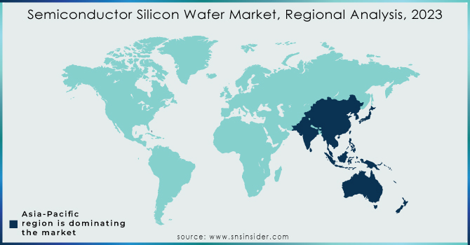
Semiconductor Silicon Wafer Market Regional Analysis
Asia Pacific dominated the market share of 35.4% in 2023 and is expected to grow at the fastest CAGR from 2024 to 2032. The increase is attributed to the presence of major semiconductor manufacturing hubs in the region, including China, Taiwan, South Korea, and Japan. This includes giant semiconductor foundries like Taiwan Semiconductor Manufacturing Company (TSMC) and SMIC, just to name two of the biggest players on the global chip production stage. Government initiatives to promote domestic semiconductor manufacturing like "Made in China 2025" of China and the Semicon India Program of India further consolidate the power of the region. The growth of the consumer electronics, automotive, and telecommunications sectors in Asia Pacific is further contributing to the demand for the semiconductor silicon wafer market. SMC investing USD 40 billion in additional chip fab capacity in Taiwan, and Samsung pledging USD 230 billion to build a semiconductor mega-cluster in Korea. Application Youri Bey, a semiconductor supply chain analyst, describes this broad application area as a growing significance of the region in the global semiconductor supply chain, as evidenced by India's tie-up with co-production with companies like Foxconn and also Micron Technology to set up semiconductor fabrication plants.
Get Customized Report as Per Your Business Requirement - Request For Customized Report
Semiconductor Silicon Wafer Companies are:
-
Shin-Etsu Chemical Co. (Polished Silicon Wafers, Epitaxial Wafers)
-
Sumco Corporation (Single Crystal Silicon Ingots, Epitaxial Wafers)
-
GlobalWafers Co., Ltd. (Polished Wafers, Silicon-On-Insulator Wafers)
-
Siltronic AG (Polished Wafers, Epitaxial Wafers)
-
SK Siltron Co., Ltd. (Silicon Wafers, Silicon Carbide Wafers)
-
Okmetic Oy (Silicon-On-Insulator Wafers, High-Resistivity RFSi Wafers)
-
Wafer Works Corporation (Polished Wafers, Epitaxial Wafers)
-
Shanghai Simgui Technology Co., Ltd. (Silicon-On-Insulator Wafers, Epitaxial Wafers)
-
Virginia Semiconductor, Inc. (Prime Silicon Substrates, SOI Substrates)
-
Tokuyama Corporation (High-Purity Polycrystalline Silicon, Silicon Wafers)
-
Elkem (Silicon Wafers, Silicon-Based Advanced Materials)
-
MEMC Electronic Materials (now SunEdison Semiconductor) (Silicon Wafers, Solar Materials)
-
Wuxi Xinte Silicon Industry Co., Ltd. (Polysilicon, Silicon Wafers)
-
DKK Dowa Electronics Co., Ltd. (Electronic Components, Silicon Materials)
-
AEM Deposition (Silicon Wafers, Silicon Carbide Wafers)
Recent Trends
-
In November 2024, Wafer Works launched a 12-inch semiconductor fab in Taiwan to meet the growing demand for AI and EV chips, with a monthly capacity of 200,000 units.
| Report Attributes | Details |
|---|---|
| Market Size in 2023 | USD 14.16 Billion |
| Market Size by 2032 | USD 22.61 Billion |
| CAGR | CAGR of 5.37% From 2024 to 2032 |
| Base Year | 2023 |
| Forecast Period | 2024-2032 |
| Historical Data | 2020-2022 |
| Report Scope & Coverage | Market Size, Segments Analysis, Competitive Landscape, Regional Analysis, DROC & SWOT Analysis, Forecast Outlook |
| Key Segments | • By Size (0-100 mm, 100-200 mm, 200- 300 mm, More than 300 mm) • By Type (N-type, P-type) • By Application (Solar Cells, Photoelectric Cells, Integrated Circuits, Others) • By End Use (Consumer Electronics, Automotive, Industrial, Telecommunications, Others) |
| Regional Analysis/Coverage | North America (US, Canada, Mexico), Europe (Eastern Europe [Poland, Romania, Hungary, Turkey, Rest of Eastern Europe] Western Europe] Germany, France, UK, Italy, Spain, Netherlands, Switzerland, Austria, Rest of Western Europe]), Asia Pacific (China, India, Japan, South Korea, Vietnam, Singapore, Australia, Rest of Asia Pacific), Middle East & Africa (Middle East [UAE, Egypt, Saudi Arabia, Qatar, Rest of Middle East], Africa [Nigeria, South Africa, Rest of Africa], Latin America (Brazil, Argentina, Colombia, Rest of Latin America) |
| Company Profiles | Shin-Etsu Chemical Co., Sumco Corporation, GlobalWafers Co., Ltd., Siltronic AG, SK Siltron Co., Ltd., Okmetic Oy, Wafer Works Corporation, Shanghai Simgui Technology Co., Ltd., Virginia Semiconductor, Inc., Tokuyama Corporation, Elkem, MEMC Electronic Materials (now SunEdison Semiconductor), Wuxi Xinte Silicon Industry Co., Ltd., DKK Dowa Electronics Co., Ltd., AEM Deposition. |
Get in Touch
