FOUP/FOSB Latch Mechanism Market Report Scope & Overview:
The FOUP/FOSB Latch Mechanism Market size was valued at USD 4.71 Billion in 2025 and is projected to reach USD 10.01 Billion by 2035, growing at a CAGR of 7.83%during 2026–2035.
The FOUP/FOSB latch mechanism market is expanding due to the critical role of 300 mm wafer carriers in semiconductor fabs. These carriers demand precise, durable latch systems to ensure contamination-free handling, seamless integration with automated material handling systems, and reliable docking at load ports. Key factors driving market growth include kinematic coupling for robotic precision, static-dissipative materials for ESD protection, moisture and purge control, and consistent weight distribution for safe automated transport. As fabs adopt higher automation levels and advanced process nodes, manufacturers providing high-quality, reliable, and adaptable latch mechanisms are poised to capture increasing demand and support operational efficiency.
Jan 21, 2026: 300 mm wafer carriers, including FOUPs and FOSBs, are critical for contamination-free handling, featuring precise kinematic coupling, reliable latches, static-dissipative materials, moisture control, and consistent weight to ensure automated fab efficiency.
FOUP/FOSB Latch Mechanism Market Size and Growth Projection:
-
Market Size in 2025: USD 4.71 Billion
-
Market Size by 2035: USD 10.01 Billion
-
CAGR (2026–2035): 7.83%
-
Base Year: 2025
-
Forecast Period: 2026–2035
-
Historical Data: 2022–2024

To Get more information On FOUP FOSB Latch Mechanism Market - Request Free Sample Report
FOUP/FOSB Latch Mechanism Market Highlights:
-
Rising Semiconductor Production: Increasing wafer fabrication and packaging volumes globally are driving demand for FOUP and FOSB latch mechanisms.
-
Automation Integration: High adoption of automated material handling systems (AMHS) and EFEMs requires precise, contamination-free latch mechanisms.
-
Diverse Wafer Compatibility: Load ports need to accommodate multiple wafer sizes (150 mm, 200 mm, 300 mm), boosting demand for adaptable latch solutions.
-
Material & Design Innovation: Growth in mechanical, spring-loaded, and precision-engineered latches enhances durability, efficiency, and scalability.
-
Regional Expansion: Asia-Pacific dominates the market due to large-scale fab operations, while North America and Europe show steady growth.
-
FOUP vs FOSB Usage: FOUPs dominate in automated fabs, while FOSBs are increasingly adopted for storage, transport, and pilot lines.
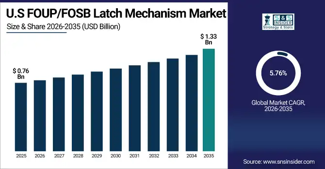
The U.S. FOUP/FOSB Latch Mechanism Market size was valued at USD 0.76 Billion in 2025 and is projected to reach USD 1.33 Billion by 2035, growing at a CAGR of 5.76% during 2026–2035, The growth of the U.S. FOUP/FOSB latch mechanism market is driven by increasing semiconductor fabrication capacity, rising adoption of advanced automation, and the need for contamination-free wafer handling. Expansion of domestic fabs and upgrades to existing facilities fuel demand for high-precision FOUP and FOSB systems. Manufacturers offering reliable, scalable, and automation-compatible latch mechanisms are positioned to benefit from rising wafer production volumes and the ongoing modernization of semiconductor manufacturing infrastructure.
FOUP/FOSB Latch Mechanism Market Drivers:
-
Diverse Wafer Carrier Designs Drive Demand for Adaptable Load Ports
The diversity of wafer carrier types, including FOUPs and FOSBs, is a key driver for the FOUP/FOSB latch mechanism market. FOUPs require fully automated, contamination-free handling for high-volume semiconductor production, while FOSBs are designed for semi-automated or manual operations, often used in storage, transport, or pilot lines. This variation creates a critical need for adaptable load ports that can accommodate multiple wafer sizes, including 150 mm, 200 mm, and 300 mm, and integrate with automated material handling systems. Manufacturers offering high-precision, flexible, and scalable latch mechanisms are positioned to capitalize on growing semiconductor fab requirements and operational efficiency demands.
Nov 04, 2025: FOUPs are fully automated 300 mm wafer carriers for in-fab handling, while FOSBs are simpler, semi-automated or manual carriers, driving the need for adaptable Load Port designs across 150 mm, 200 mm, and 300 mm wafers.
FOUP/FOSB Latch Mechanism Market Restraints:
-
High Manufacturing Costs and Design Complexity Hinder FOUP/FOSB Latch Mechanism Adoption
High manufacturing and material costs make advanced FOUP and FOSB systems expensive for fabs, particularly small and mid-sized facilities. The complexity of precision-engineered latch designs, coupled with strict contamination control requirements, increases production and maintenance challenges. Integration with automated wafer handling systems requires skilled personnel and advanced infrastructure, creating additional barriers. Furthermore, supply chain disruptions and dependency on specialized components can delay deployment. These factors collectively restrain rapid adoption, slowing market expansion despite growing demand for high-volume, contamination-free semiconductor wafer transport solutions.
FOUP/FOSB Latch Mechanism Market Opportunities:
-
Rising Semiconductor Automation Drives Growth in FOUP/FOSB Latch Mechanism Market
The FOUP/FOSB latch mechanism market presents substantial growth potential driven by increasing semiconductor fabrication, rising automation, and demand for contamination-free wafer handling solutions. As fabs worldwide scale production to meet advanced node requirements, the need for reliable, high-precision FOUP and FOSB systems intensifies. This creates opportunities for manufacturers to innovate in mechanical, spring-loaded, and precision-engineered latch designs, enhance durability, and improve integration with automated wafer handling processes. Companies offering technologically advanced, scalable, and quality-driven solutions can capture market share, establish strategic partnerships with semiconductor fabs, and support the global push for efficient, high-volume wafer production.
Taiwan continues to lead global 300 mm FOUP demand, with Taiwanese fabs accounting for about 65 % of worldwide 300 mm FOUP usage, driven by massive investments in advanced nodes and automation to support foundries and packaging operations
FOUP/FOSB Latch Mechanism Market Segment Highlights:
-
By Latch Type: Dominant – Mechanical Latch Mechanisms (54.50% → 50.50%); Fastest-Growing – Spring-Loaded Latch Systems (26.00% → 34.00%, CAGR 10.72%)
-
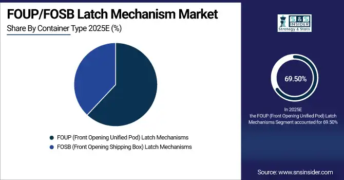
By Container Type: Dominant – FOUP (Front Opening Unified Pod) Latch Mechanisms (69.50% → 65.50%); Fastest-Growing – FOSB (Front Opening Shipping Box) Latch Mechanisms (30.50% → 34.50%, CAGR 9.16%)
-
By Wafer Size Compatibility: Dominant – 300 mm (64.50% → 60.45%); Fastest-Growing – Above 300 mm (21.50% → 29.15%, CAGR 11.11%)
-
By End-Use Application: Dominant – Semiconductor Fabrication Plants (Wafer Fabs) (59.40% → 54.60%); Fastest-Growing – Semiconductor Packaging & Testing Facilities (15.40% → 18.60%, CAGR 9.86%)
By Latch Type: Mechanical Latch Mechanisms Dominating and Spring-Loaded Latch Systems Fastest-Growing
Mechanical Latch Mechanisms remain the dominant latch type in the FOUP/FOSB Latch Mechanism market, driven by their reliability, simplicity, and widespread adoption in semiconductor fabs. Spring-Loaded Latch Systems are the fastest-growing segment, supported by increasing demand for automated, high-precision, and contamination-free wafer handling solutions.
By Container Type: FOUP Dominating and FOSB Fastest-Growing
FOUP (Front Opening Unified Pod) Latch Mechanisms remain the dominant container type in the FOUP/FOSB market, driven by widespread use in wafer fabs for reliable, contamination-free handling. FOSB (Front Opening Shipping Box) Latch Mechanisms are the fastest-growing segment, supported by rising adoption in automated logistics and advanced wafer transport systems.
By Wafer Size Compatibility: 300 mm Wafer Dominating and Above 300 mm Fastest-Growing
The 300 mm wafer segment remains dominant in the FOUP/FOSB market, owing to its standardization and extensive use in semiconductor fabrication. Above 300 mm wafers are the fastest-growing segment, driven by demand for advanced nodes, larger wafer formats, and next-generation semiconductor manufacturing.
By End-Use Application: Wafer Fabs Dominating and Packaging & Testing Fastest-Growing
Semiconductor Fabrication Plants (Wafer Fabs) are the dominant end-use application, driven by high-volume wafer production and automation needs. Semiconductor Packaging & Testing Facilities are the fastest-growing segment, supported by increasing chip output, advanced packaging requirements, and adoption of precision FOUP/FOSB handling systems.
FOUP/FOSB Latch Mechanism Market Regional Highlights:
-
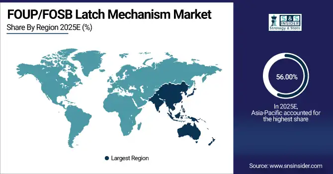
Asia-Pacific: 56.00% → 64.00% in 2035, Dominant Region and Fastest-Growing (CAGR 9.27%)
-
North America: 24.50% → 20.50% in 2035, Leading Share in 2025 with Gradual Decline (CAGR 5.91%)
-
Europe: 14.70% → 12.30% in 2035, Moderate Share with Slow Decline (CAGR 5.91%)
-
Latin America: 2.90% → 2.10% in 2035, Small Share with Moderate Decline (CAGR 4.36%)
-
Middle East & Africa: 1.90% → 1.10% in 2035, Emerging Region with Slow Growth (CAGR 1.96%)
Asia-Pacific FOUP/FOSB Latch Mechanism Market Insights:
The Asia-Pacific FOUP/FOSB Latch Mechanism market dominates globally, driven by rapid semiconductor fab expansions, increasing automation, and rising demand for high-purity wafer handling solutions. Strong investment in China, South Korea, and Japan, coupled with technological advancements and government support, positions the region as both the largest and fastest-growing market through 2035.
Get Customized Report as per Your Business Requirement - Enquiry Now
China FOUP/FOSB Latch Mechanism Market Insights:
China leads the Asia-Pacific FOUP/FOSB Latch Mechanism market, driven by massive semiconductor fabrication growth, government incentives, and increasing adoption of automated, high-precision wafer handling solutions across domestic fabs and advanced technology nodes.
North America FOUP/FOSB Latch Mechanism Market Insights:
The North America FOUP/FOSB Latch Mechanism market is experiencing robust growth, fueled by rising semiconductor manufacturing, investments under the CHIPS Act, and increasing demand for automated, contamination-free wafer handling systems in advanced fabs across the U.S. and Canada, supporting next-generation electronics and high-volume production.
U.S. FOUP/FOSB Latch Mechanism Market Insights:
The U.S. FOUP/FOSB Latch Mechanism market is expanding steadily, driven by CHIPS Act investments, growing semiconductor fabrication, and adoption of automated, high-precision wafer handling systems in advanced domestic fabs.
Europe FOUP/FOSB Latch Mechanism Market Insights:
The Europe FOUP/FOSB Latch Mechanism market is growing moderately, supported by steady semiconductor fabrication activities, adoption of automated wafer handling solutions, and investments in advanced manufacturing technologies. Germany, France, and the Netherlands lead regional demand, focusing on precision, contamination-free handling, and integration with next-generation semiconductor production lines.
Germany FOUP/FOSB Latch Mechanism Market Insights:
Germany’s FOUP/FOSB Latch Mechanism market is expanding steadily, driven by growing semiconductor manufacturing, adoption of automated wafer handling systems, and focus on high-precision, contamination-free FOUP/FOSB solutions in advanced fabs.
Latin America FOUP/FOSB Latch Mechanism Market Insights:
The Latin America FOUP/FOSB Latch Mechanism market is witnessing steady growth, driven by gradual expansion of semiconductor manufacturing, increased adoption of automated wafer handling solutions, and rising investments in advanced fab infrastructure across countries like Brazil and Mexico, supporting regional demand for high-precision FOUP and FOSB systems.
Brazil FOUP/FOSB Latch Mechanism Market Insights:
Brazil is the dominant country in the FOUP/FOSB Latch Mechanism market, driven by growing semiconductor manufacturing, increasing automation adoption, and investments in advanced wafer handling solutions to support regional fabs.
Middle East & Africa (MEA) FOUP/FOSB Latch Mechanism Market Insights:
The Middle East & Africa FOUP/FOSB Latch Mechanism market is growing gradually, supported by emerging semiconductor fabrication projects, increasing investments in automation and wafer handling infrastructure, and adoption of high-precision FOUP and FOSB systems in countries focusing on electronics manufacturing and technological development.
United Arab Emirates FOUP/FOSB Latch Mechanism Market Insights:
The United Arab Emirates (UAE) is the dominant country, driven by government-backed semiconductor initiatives, advanced industrial infrastructure, and strategic investments in electronics manufacturing hubs.
FOUP/FOSB Latch Mechanism Market Competitive Landscape:
Entegris, Inc. (established in 1966) is a U.S.-based company specializing in advanced materials, contamination control, and wafer handling solutions for the semiconductor industry. It provides FOUPs, FOSBs, filtration, and chemical delivery systems, enabling high-purity, automated, and reliable semiconductor manufacturing across global fabs.
-
In Dec 2024, Entegris and U.S. Department of Commerce Announce Entry Into Award Agreement Under CHIPS Act– definitive agreement providing up to USD 77 million CHIPS Act funding to build a state‑of‑the‑art manufacturing center in Colorado Springs that will support production of semiconductor wafer carriers (FOUPs) and advanced materials
FOUP/FOSB Latch Mechanism Companies are:
-
Entegris, Inc.
-
Brooks Automation, Inc.
-
Tokyo Electron Limited (TEL)
-
KLA Corporation
-
ASM Pacific Technology Limited
-
Hitachi High-Tech Corporation
-
Panasonic Corporation
-
Nikon Corporation
-
Canon Tokki Corporation
-
AMAT Automation Solutions
-
Ebara Corporation
-
Teradyne, Inc.
-
SEMI Equipment Suppliers (Tier-1 consortium)
-
Nissin Electric Co., Ltd.
-
Advantest Corporation
-
Lam Research Corporation
-
Veeco Instruments Inc.
-
TSMC Automation Partners
| Report Attributes | Details |
|---|---|
| Market Size in 2025 | USD 4.71 Billion |
| Market Size by 2035 | USD 10.01 Billion |
| CAGR | CAGR of 7.83% From 2026 to 2035 |
| Base Year | 2025 |
| Forecast Period | 2026-2035 |
| Historical Data | 2022-2024 |
| Report Scope & Coverage | Market Size, Segments Analysis, Competitive Landscape, Regional Analysis, DROC & SWOT Analysis, Forecast Outlook |
| Key Segments | • By Latch Type(Mechanical Latch Mechanisms, Spring-Loaded Latch Systems, Cam-Based / Rotary Latch Mechanisms and Hybrid & Precision-Engineered Latches) • By Container Type(FOUP (Front Opening Unified Pod) Latch Mechanisms and FOSB (Front Opening Shipping Box) Latch Mechanisms) • By Wafer Size Compatibility (Up to 200 mm, 300 mm, Above 300 mm (Emerging / Advanced Nodes)) • By End-Use Application(Semiconductor Fabrication Plants (Wafer Fabs), Semiconductor Packaging & Testing Facilities, Wafer Logistics & Storage Systems and Equipment OEMs & Automation Integrators) |
| Regional Analysis/Coverage | North America (US, Canada), Europe (Germany, UK, France, Italy, Spain, Russia, Poland, Rest of Europe), Asia Pacific (China, India, Japan, South Korea, Australia, ASEAN Countries, Rest of Asia Pacific), Middle East & Africa (UAE, Saudi Arabia, Qatar, South Africa, Rest of Middle East & Africa), Latin America (Brazil, Argentina, Mexico, Colombia, Rest of Latin America). |
| Company Profiles | Key players in the FOUP/FOSB Latch Mechanism market include Entegris, Inc., MKS Instruments, Inc., Brooks Automation, Inc., Tokyo Electron Limited (TEL), KLA Corporation, Applied Materials, Inc., ASM Pacific Technology Limited, Hitachi High-Tech Corporation, Panasonic Corporation, Nikon Corporation, Canon Tokki Corporation, AMAT Automation Solutions, Ebara Corporation, Teradyne, Inc., SEMI Equipment Suppliers (Tier-1 consortium), Nissin Electric Co., Ltd., Advantest Corporation, Lam Research Corporation, Veeco Instruments Inc., and TSMC Automation Partners. |
Frequently Asked Questions
Asia-Pacific dominated the FOUP/FOSB Latch Mechanism Market in 2025.
The “Mechanical Latch Mechanisms” segment dominated during the projected period.
Key drivers of the FOUP/FOSB Latch Mechanism Market include increasing semiconductor wafer fabrication, demand for automation in fabs, need for precision and contamination-free handling, and adoption of advanced lithography and packaging technologies.
The FOUP/FOSB Latch Mechanism Market size was USD 4.71 Billion in 2025 and is expected to reach USD 10.01 Billion by 2035.
The FOUP/FOSB Latch Mechanism Market is expected to grow at a CAGR of 7.83% from 2026-2035.
Get in Touch
