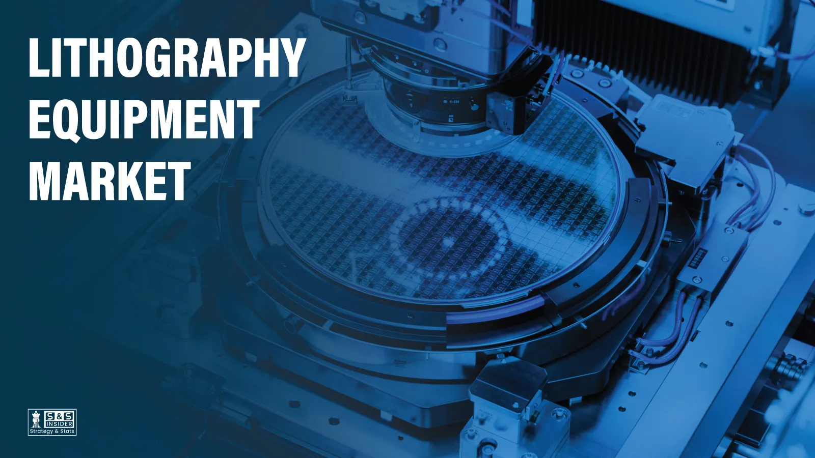
The industry of lithography equipment is on an upward trend in the world because of the increasing need for semiconductors of advanced nodes due to applications such as AI, high-performance computing, 5G and auto electronics. This is due to the fact that these machines transfer the design onto wafers using light or electrons. The increasing use of EUV lithography for below-7nm process technology is further increasing the need for these equipment.
The Lithography Equipment Market was valued at USD 28.63 billion in 2025 and is estimated to be worth USD 53.94 billion by 2035, growing at a CAGR of 6.54% during the forecast period of 2026 to 2035. ArF Immersion accounted for 49.20% technology share in 2025, whereas the fastest growing technology is EUV with a CAGR of 8.99%.
Regional Analysis of the Lithography Equipment Market
The global market for lithography equipment is witnessing growth in the Asia-Pacific, North America, Europe, South America, and Middle East & Africa regions. Asia-Pacific dominated the largest share of 45.50% in 2025, while being the fastest-growing region due to high semiconductor fabrication capacities and investments in China, Taiwan, South Korea, and Japan. In the US market, the lithography equipment market value reached USD 4.53 billion in 2025 and forecasted to grow to USD 7.69 billion by 2035 at a CAGR of 5.43%.
North America holds the 23.90% market share in 2025 and is growing at a CAGR of 6.18%, backed by the demand from AI applications, data centers, and defense. Europe shows steady growth at a CAGR of 6.05%, driven by the automotive semiconductor demand, industrial automation, and EU Chips Act, where Germany, France, and the Netherlands are the key economies. South America and Middle East & Africa are the emerging regions with slow growth due to expanding electronics assembly and digital infrastructure.
Top 10 Trends in the Lithography Equipment Market
-
AI, HPC, 5G, and automotive demand: Rapid growth in AI, high-performance computing, 5G, automotive electronics, and IoT devices is driving equipment demand.
-
EUV lithography: It enables advanced node scaling below 7nm for next-generation chips.
-
ArF immersion lithography: It remains dominant in high-volume production fabs.
-
Electron beam lithography: It is gaining traction in R&D and mask manufacturing applications.
-
Advanced packaging: Chiplets and heterogeneous integration are increasing lithography usage intensity.
-
Rising chip complexity: More complex semiconductors need higher resolution and precision tools.
-
Extreme miniaturization: Shrinking features are increasing adoption of next-generation lithography systems.
-
High-NA EUV: Chipmakers are moving toward systems that support sub-2nm manufacturing, as seen in the ASML and imec test laboratory.
-
Automotive chips: The automotive industry is the fastest-growing end use at a CAGR of 8.44%, supported by EV adoption and ADAS.
-
Government and fab investment: Domestic fabrication programs in the United States, Europe, and China are lifting equipment demand.
Unlock exclusive market insights download the brochure to explore global lithography equipment market trends, emerging opportunities, competitive developments, and forecasts through 2035
Lithography Equipment Market Growth Drivers and Opportunities
EUV technology along with High-NA EUV technology is one of the major markets drivers. There is a need for systems that can allow creating sub-5 nm and sub-2 nm nodes for AI, high-performance computing, and new generation data centers. Growing chip complexity is increasing the need for advanced high-resolution patterning, cleaning, and inspection. SCREEN Holdings and IBM enhanced cooperation in wafer cleaning in September 2025 for use in the EUV and High-NA EUV lithography. The advanced packaging accounted for an application share of 35.70% in 2025.
There are many opportunities in areas like AI, cloud computing, automotive electronics, and in data center segments where the designs of chips require precise patterning. Nikon introduced the DSP-100 Digital Lithography System in 2026. In March 2026, Lace Lithography announced securing €34.5 million to develop atom-based BEUV systems. Challenges include very expensive investment cost of EUV systems, supply issues, limited number of players, and technical limitations at sub-5 nm nodes. Geopolitical tensions and export controls can be seen among challenges too. Nevertheless, there is going to be market growth until 2035 because of the needs for AI chips.
Top 10 Companies Leading the Lithography Equipment Market
-
ASML
-
Nikon
-
SCREEN Holdings
-
Canon
-
Applied Materials
-
Lam Research
-
Tokyo Electron
-
KLA
-
SUSS MicroTec
-
EV Group
Unlock exclusive market insights request the free sample report to delve into the global lithography equipment market.
1. ASML
 ASML is a company that was founded in 1984 and produces lithography tools. ASML collaborated with imec to create a High-NA EUV test laboratory. In June 2024, the laboratory was inaugurated in Veldhoven, Netherlands. The laboratory allows manufacturers and suppliers to test sub-2nm technology. Intel acquired the ASML’s TWINSCAN EXE:5200B, which was the first High-NA EUV machine, in December 2025.
2. Nikon
 Nikon is a Japan-based precision equipment manufacturer and also supplies lithography equipment to companies. It provides equipment to semiconductor firms which require precise patterns transfer for high-end chips and packaging. In 2026, it came up with the DSP-100 Digital Lithography System to help facilitate the fabrication of next generation semiconductors due to the growing need for AI, cloud, and data centers.
3. SCREEN Holdings
 SCREEN Holdings is a semiconductor equipment maker based in Japan providing wafer cleaning solutions in combination with lithography. Wafer cleaning and inspection become crucial due to the increasing complexity of chip architecture. In September 2025, it intensified its collaboration with IBM with the aim of developing wafer cleaning techniques to support EUV and High-NA EUV lithography.
4. Canon
 Canon is a Japan-based imaging and optical products manufacturer that provides lithography equipment to semiconductor companies. The company is listed as one of the key players in the global lithography equipment market. One of its business units, Canon Nanotechnologies, which is also listed in the list of the key players, is working on an alternative patterning technique for making chips known as nanoimprint lithography.
5. Applied Materials
 Applied Materials is a US-based supplier of semiconductor equipment and a key player in the lithography equipment market. Its equipment is involved in processes surrounding the exposure process, such as deposition, etching, and inspection of the chips, becoming increasingly complex with increased complexity of chip architectures and chiplets.
Company Profile
1. ASML
-
Business Overview
-
Company Snapshot
-
Product Overview
-
Company Market Share Analysis
-
Company Coverage Portfolio
-
Financial Analysis
-
Recent Developments
-
Mergers and Acquisitions
-
SWOT Analysis
2. Nikon
3. SCREEN Holdings
4. Canon
5. Applied Materials
6. Lam Research
7. Tokyo Electron
8. KLA
9. SUSS MicroTec
10. EV Group
Future Outlook of the Lithography Equipment Market
Lithography tool industry is likely to grow at a fast pace owing to the continued requirement for advanced chips used in AI, HPC, 5G, and automotive electronics. The adoption of EUV and High-NA EUV tools, along with the growth in advanced packaging and electron beam patterning, has created new opportunities for tool vendors. Fab investments in Asia-Pacific region and chip initiatives in other regions will ensure high demand. The vendors that will gain from it will be those providing high resolution, reliable, and cost-effective patterning tools.