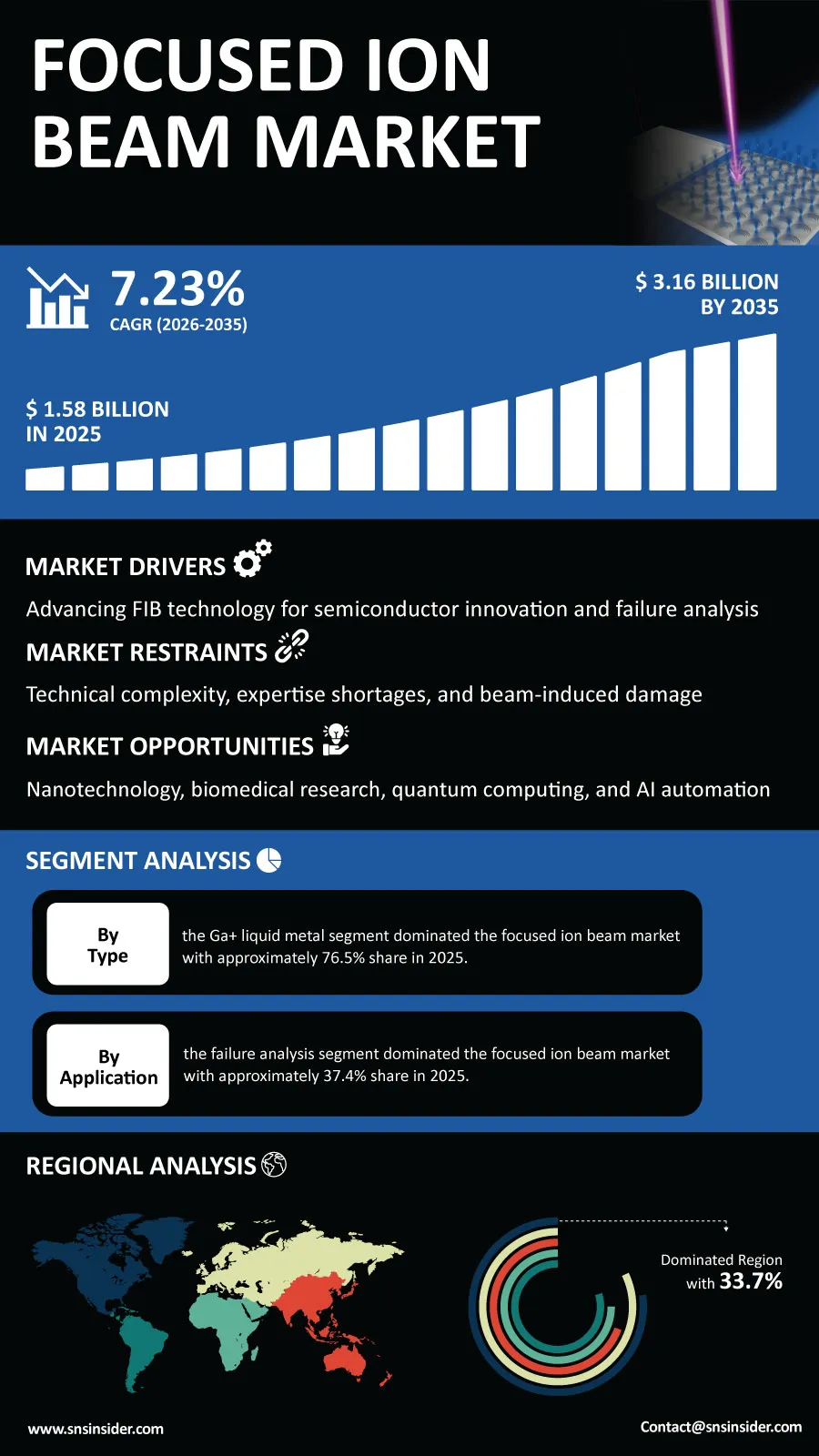
The global Focused Ion Beam Market is entering a period of sustained expansion as semiconductor manufacturers, research laboratories, and advanced technology companies increase investments in nanoscale analysis and precision material processing. According to a recent study by SNS Insider, the global Focused Ion Beam Market size valued at USD 1.58 billion in 2025, is anticipated to grow to USD 3.16 billion by 2035, registering a CAGR of 7.23% over the 2026–2035 forecast period.
The ever-shrinking size of electronic parts is driving the demand for analytical solutions that can analyze and manipulate structures on an ultrasmall scale. The use of FIB solutions in the development of semiconductors, failure analysis, sample preparation, and advanced materials is gaining significance for applications where high precision and controlled material processing are essential.
Investment in the development of artificial intelligence, quantum computing, advanced packaging, and nanotechnology will continue to expand the target markets. Equipment makers are introducing automation solutions, better visualization systems, and FIB-SEM solutions to boost efficiency and eliminate the reliance on highly skilled operators.
To Get Detailed Insights on the Focused Ion Beam Market – Request a Sample Report
Semiconductor Complexity and Automation Create New Growth Opportunities
Fast-paced developments in the field of advanced semiconductors have led to the growing need for efficient and accurate equipment capable of defect identification, isolation, and preparation for further inspection. With the transition of manufacturers to increasingly complex process nodes, the traditional approach to failure analysis becomes inadequate, thus reinforcing the importance of FIB systems in both scientific and production labs.
Automation has also become one of the most significant competitive advantages. With the help of artificial intelligence, it will be possible to automate routine processes of samples' preparation and lamellas' cutting, increasing laboratories' efficiency while minimizing human involvement. In addition, plasma-based FIB systems provide an extended application range due to faster material removal.
Emerging fields including quantum computing, photonics, biomedical engineering, and advanced materials are creating additional opportunities for FIB technology as researchers seek precise nanoscale fabrication and characterization capabilities.
Key Market Insights Highlight Shifting Demand Patterns
By type, Ga+ liquid metal systems are expected to account for approximately 76.5% of global market revenue in 2025, supported by their established use in semiconductor failure analysis, circuit modification, imaging, and nanoscale processing. Gas field ion source systems are projected to record the fastest growth through 2035 as demand rises for ultra-high-resolution analysis and applications requiring enhanced surface sensitivity.
Based on application, failure analysis is anticipated to represent approximately 37.4% of market revenue in 2025. The segment continues to benefit from the increasing complexity of integrated circuits and the need to identify defects, investigate failures, and improve semiconductor reliability. Nanofabrication is expected to experience the fastest growth as FIB systems gain traction in quantum computing, photonics, sensors, and next-generation material development.
By vertical, electronics and semiconductor applications are projected to dominate the market with approximately 51.4% of revenue in 2025. Rising investment in advanced chip manufacturing, packaging technologies, and high-performance computing is expected to maintain strong demand for FIB systems across the sector.
AI-Enabled Workflows Expand the Role of FIB Systems
The combination of artificial intelligence and automation is changing the way FIBs function through enhancing repeatability and decreasing the need for human interaction during complicated processes. Automated procedures are allowing laboratories to speed up sample and analysis preparation while solving the problem of a lack of highly skilled FIB operators.
Moreover, FIBs have been found useful in such areas as counterfeit electronics analysis, aerospace investigations, military research, and material science. Their usage in those spheres will most likely become more common as organizations become more interested in detailed forensic investigation of complex electronic and material systems.
North America Leads with 33.7% Market Share as China Contributes 40.6% of Asia Pacific Revenue
North America will continue to dominate the regional market share, with an estimated revenue share of about 33.7% in 2025. This region is favored due to its robust semiconductor eco-system, presence of well-established research facilities and concentration of scientific establishments and technology-based companies. The United States contributes around 82.5% of the total revenue share in North America, fueled by investments in semiconductors and government-funded research initiatives.
The Asia Pacific region will have the highest growth rate between 2015 and 2035. Semiconductors, electronics, and the research on nanotechnology are creating a favorable environment for the growth of this market. China contributes about 40.6% of the total regional revenue, and semiconductor development in Japan, South Korea, Taiwan, and India is anticipated to bolster the demand.
Industry Participants Focus on Automation and Advanced Beam Technology
The competitive landscape is evolving as leading manufacturers prioritize automation, multi-beam capabilities, plasma FIB systems, and integrated analytical platforms. Companies are increasingly focused on improving throughput, simplifying complex workflows, and expanding FIB applications beyond conventional semiconductor analysis.
Key companies operating in the global Focused Ion Beam Market include Thermo Fisher Scientific Inc., ZEISS International, Hitachi High-Tech Corporation, JEOL Ltd., TESCAN ORSAY HOLDING, a.s., Raith GmbH, A&D Company, Limited, Veeco Instruments Inc., Eurofins Scientific, Delong Instruments a.s., Fibics Incorporated, Zyvex Labs LLC, Ionoptika Ltd., Nanosurf AG, Oxford Instruments plc, Orsay Physics, Bruker Corporation, Fischione Instruments, Inc., Applied Nanotools Inc., and GETec Microscopy GmbH.
An SNS Insider analyst Sushant Kadam commented, “The growing complexity of semiconductor devices and accelerating investment in nanoscale technologies are strengthening demand for precision ion beam systems. As automation, AI-assisted workflows, and advanced beam technologies mature, FIB platforms are expected to become increasingly accessible to a broader range of industrial and research users, creating new opportunities across semiconductor, quantum, biomedical, and materials science applications.”
About the Author

Get in touch