Focused Ion Beam Market Report Scope & Overview:
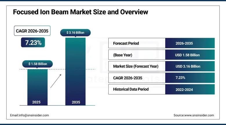
The Focused Ion Beam Market size was USD 1.58 Billion in 2025 and is expected to reach USD 3.16 Billion by 2035, growing at a CAGR of 7.23% from 2026–2035.
The Focused Ion Beam (FIB) market is currently witnessing rapid growth owing to factors such as an increase in intricacies associated with semiconductor processing technologies, growing need for effective failure analysis, and increasing applications in the field of nanotechnology research. Due to the growing investments made by semiconductor manufacturing companies in the fabrication of advanced nodes and better yield from their processes, there has been increasing demand for high precision FIB equipment that is used for tasks such as circuit editing, defect localization, sample preparation, and material analysis. There are continued developments being made in order to increase the precision of FIB equipment, enhance imaging, automate processes, and improve nanoscale processing.
Thermo Fisher Scientific, ZEISS International, and Hitachi High-Tech represent some of the industry giants contributing to the growth of the FIB-SEM technology through automation and AI-based processes. FIB with significantly faster removal rate compared to the standard Ga+ tools is increasingly used in high-throughput analysis of semiconductors and package failure analysis. The technology of FIB is gaining more relevance in the field of quantum computing research due to the ability to achieve accurate patterning of qubits. In the United States, institutions such as NASA and universities conduct research related to space nanofabrication and material science using the technology of FIB. All these factors of demand in various industries contribute to the growth of the FIB market.
Market Size and Forecast
-
Market Size in 2026E: USD 1.69 Billion
-
Market Size by 2035: USD 3.16 Billion
-
CAGR: 7.23% from 2026 to 2035
-
Fastest Growing Region: Asia Pacific
-
Largest Region: North America (33.7%)
To Get more information On Focused Ion Beam Market - Request Free Sample Report
Focused Ion Beam Market Trends
-
Plasma FIB adoption is accelerating for high-throughput cross-section preparation and large-area material removal.
-
AI-driven automation in FIB-SEM systems is enabling hands-free lamella preparation and autonomous failure analysis.
-
Multi-beam FIB systems combining ion and electron beams are enabling faster, more comprehensive sample characterization.
-
Quantum computing research is creating new demand for FIB nanofabrication of sub-10nm device structures.
-
FIB integration with advanced analytical tools including EBSD and EDS is expanding material characterization capability.
-
Counterfeit electronics detection using FIB is gaining regulatory and defense sector momentum globally.
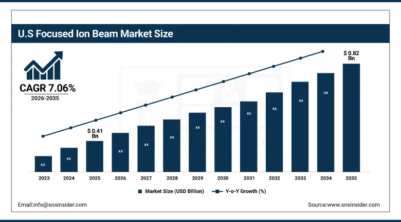
The U.S. Focused Ion Beam Market Outlook
The U.S. Focused Ion Beam Market was valued at approximately USD 0.41 Billion in 2025. It is expected to reach approximately USD 0.82 Billion by 2035, growing at a CAGR of approximately 7.06%.
The U.S. market is witnessing immense growth due to development of the semiconductor and electronics markets. FIB equipment is widely employed for failure analysis, nanofabrication, and manipulation in America’s extensive semiconductor industry landscape. As semiconductor devices become denser, analytical tools such as FIB are in increasing demand to characterize materials and defects. Greater use in the fields of aerospace, defense, and biomedical research, as well as developments in multi-beam FIB and plasma FIB techniques, are adding fuel to the fire. The detection of counterfeit electronics in the American defense market constitutes one such value-added area.
In October 2024, ZEISS launched the Crossbeam 550 Samplefab FIB-SEM, an automated system for high-precision TEM sample preparation. The system enables hands-free lamella production with over 90% automation yield, dramatically reducing skilled operator time. This kind of automation milestone reflects the broader industry shift toward reducing the skill barrier for FIB operation. As FIB automation keeps advancing, adoption should expand beyond large research institutions into mid-size semiconductor manufacturers. Similar automated FIB platforms are likely to follow from competing vendors as automation becomes a key differentiation axis. These developments directly address the skilled personnel shortage that has historically limited FIB market penetration.
Focused Ion Beam Market Segment Analysis
-
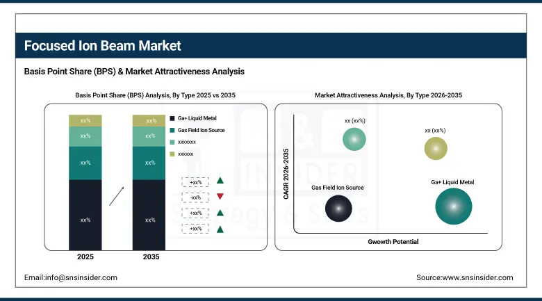
By Type, the Ga+ liquid metal segment dominated the focused ion beam market with approximately 76.5% share in 2025. The gas field ion source segment is expected to witness the highest CAGR through the forecast period.
-
By Application, the failure analysis segment dominated the focused ion beam market with approximately 37.4% share in 2025. The nanofabrication segment is expected to grow at the highest CAGR during the forecast period.
-
By Vertical, the electronics & semiconductor segment dominated the focused ion beam market with approximately 51.4% share in 2025 and is also anticipated to expand at an impressive CAGR through the forecast period.
By Type, Ga+ dominates on established precision, Gas Field grows fastest
The Ga+ liquid metal FIB was the most prominent type of system in 2025 with an estimated market share of 76.5%. The high accuracy, stability, and popularity of this type of system in semiconductor failure analysis, circuit editing, and nanofabrication is what accounts for its prominence. Due to the depth of focus and thinness of the ion beam, Ga+ FIBs can be used for many high resolution imaging, milling, and deposition applications both in research and industry. They provide focused ion beams that can remove and modify materials with utmost accuracy, which makes them crucial in research and industry environments.
Gas Field Ion Sources are anticipated to register the highest CAGR during the forecast period. These sources have been gaining popularity because of their high resolution, high surface sensitivity, and reduced sample damage as compared to Ga+ FIB. The applications of Gas Field technology are creating an impact in nanotechnology, defect analysis, and state-of-the-art projects that require ultra-high precision. Increased investment in advanced semiconductor devices and miniaturization of components is driving the Gas Field FIB market. Plasma FIB completes the types list, providing increased material removal rates.
By Application, failure analysis dominates, nanofabrication grows fastest
Failure Analysis accounted for the largest application share of approximately 37.4% in 2025. This dominance is driven by FIB's importance in the semiconductor and electronics industry for defect detection, fault isolation, and material characterization. As semiconductor devices shrink into higher technology nodes, failure analysis through FIB remains a vital component for quality assurance, reliability, and product optimization. The precision of FIB failure analysis is especially critical for complex integrated circuits and MEMS/NEMS devices where defect dimensions are at or below the nanometer scale. Circuit editing and device modification also contribute meaningfully as established FIB application categories.
The nanofabrication segment is expected to grow at the highest CAGR through the forecast period. Its increasing applications in quantum computing, photonics, and biomedical research drive this rapid expansion. FIB-based nanofabrication relies on precise modification and nano-patterning of materials, making it essential for next-generation chips, sensors, and nanostructured materials. Rising nanotechnology-based innovations will expedite FIB adoption in advanced material research and manufacturing. Counterfeit detection is also growing as a specialized FIB application in defense and security.
Regional Analysis
|
Region |
Major Country |
Share within Region, 2025 (%) |
|---|---|---|
|
North America |
United States |
82.5% |
|
Europe |
Germany |
24.6% |
|
Asia Pacific |
China |
40.6% |
|
Middle East & Africa |
UAE |
22.8% |
|
Latin America |
Brazil |
43.8% |
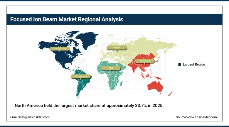
North America Focused Ion Beam Market Insights
North America held the largest market share of approximately 33.7% in 2025 for Focused Ion Beam systems. High concentration of key semiconductor companies, research institutes, and nanotechnology centers in the region drives this leadership. Thermo Fisher Scientific, Intel, and IBM are among the active users of FIB for failure analysis, circuit modification, and material research. NASA and top universities also use FIB for space-related nanofabrication and material science advancement. The aerospace and defense sector drives additional demand through counterfeit detection and microelectronics analysis.
The United States accounts for approximately 82.5% of North American revenue. Government-funded research programs and growing semiconductor manufacturing investment both reinforce domestic FIB demand. This combination of commercial semiconductor use and research institution demand keeps North America firmly in the lead.
Get Customized Report as per Your Business Requirement - Enquiry Now
Europe Focused Ion Beam Market Insights
Europe represents a meaningful FIB market, supported by strong academic research and precision manufacturing investment. Germany leads the regional market, backed by strong semiconductor research institutions and materials science investment. France and the UK contribute meaningful demand through their own expanding academic and industrial research sectors.
Germany accounts for approximately 24.6% of European revenue. Fraunhofer and Max Planck institutes are among the leading European academic users of FIB for materials research and semiconductor analysis. This research infrastructure keeps supporting steady European market growth.
Asia Pacific Focused Ion Beam Market Insights
Asia Pacific is expected to register the fastest growth from 2026 to 2035. Rapid developments in semiconductor production, consumer electronics, and nanotechnology studies all drive this expansion. Semiconductor giants including TSMC, Samsung, and SMIC in China, Japan, South Korea, and Taiwan are heavily investing in next-generation chip innovation and failure analysis using FIB. AI, 5G, and electric vehicle technologies keep increasing demand for circuit editing and nanofabrication-based FIB applications.
China accounts for approximately 40.6% of Asia Pacific revenue. Chinese and Indian government initiatives to bolster domestic semiconductor production are further projected to boost regional FIB adoption. As semiconductor capital investment keeps expanding regionally, this growth trajectory should continue strengthening.
MEA & Latin America Focused Ion Beam Market Insights
The UAE leads MEA revenue, growing semiconductor and electronics research investment, alongside expanding defense applications, both support regional FIB adoption. Saudi Arabia is also expanding its nanotechnology and advanced manufacturing research capacity.
Brazil leads Latin American revenue, growing materials science research and expanding semiconductor-adjacent manufacturing both drive regional demand. Mexico and Argentina contribute secondary demand through their own expanding scientific research sectors.
Market Dynamics
Growth Drivers: Advancing FIB technology for semiconductor innovation and failure analysis
Increased usage of semiconductor trends and increased demand for failure analysis, modification, and nanofabrication are driving the growth of the FIB market. With semiconductor node miniaturization and growing IC complexity, FIB has emerged as an effective technique of material extraction, defect analysis, and TEM sample preparation. Rising use of 5G, AI, and IoT devices is also increasing the demand for advanced semiconductor testing and fabrication techniques. Issues with counterfeit electronics in industries like defense, aerospace, and automotive are creating a robust demand for forensic detection through FIB.
The development of plasma FIB technology has made it possible to remove large-area materials, thus making FIB suitable for high throughput applications. Automation and AI capabilities in FIB technology are decreasing the skill barrier that had been hindering the use of FIB technology. Since the complexity of semiconductor devices keeps on increasing, this driver will persist throughout the forecast period.
Restraints: Technical complexity, expertise shortages, and beam-induced damage
Highly specialized technological complexities and operational skill set required in FIB machines represent significant limitations in FIB industry. Skilled technicians are required to control ion milling, deposition, and imaging process. The dearth of technicians continues to inhibit the growth in the market. Beam damage and alteration are other key concerns, particularly where higher accuracy analysis and nanofabrication are concerned in semiconductors.
Preservation of resolution while minimizing beam damage is a continual problem that engineers face. These technical limitations and lack of skilled labor continues to inhibit the growth of FIB market in cost sensitive regions and those lacking skilled technicians. Automated FIB system represents a promising trend overcoming the skill set limitation.
Opportunities: Nanotechnology, biomedical research, quantum computing, and AI automation
There is sufficient room for growth in nanotechnology, biomedical research, and material sciences. Introduction of FIB technology in quantum computers, MEMS/NEMS devices, and batteries will provide further growth prospects in the market. Increasing need for customized multi-scale structures in biotechnology and drug delivery systems is also broadening the scope of FIB's target market.
AI-driven automation is facilitating high efficiency and accuracy in FIB systems, leading to faster adoption by different industries. Nanofabrication using FIB technology is key to the development of future generation chips, sensors, and nano-materials in various high-growth industries. With continued advances in automation and reduction in operator burden, FIB technology will be available to more users.
Recent Developments:
-
2024: ZEISS launched the Crossbeam 550 Samplefab FIB-SEM in October 2024, an automated system for high-precision TEM sample preparation enabling hands-free lamella production with over 90% automation yield.
-
2024: Thermo Fisher Scientific introduced AI-driven automation enhancements to its FIB-SEM portfolio, including automated lamella preparation workflows targeting semiconductor failure analysis efficiency improvements.
-
2024: JEOL Ltd. expanded its multi-beam FIB capabilities with new plasma FIB configuration options designed for higher-throughput cross-section preparation in advanced semiconductor packaging research.
Focused Ion Beam Market Key Players are:
-
Thermo Fisher Scientific Inc.
-
ZEISS International
-
Hitachi High-Tech Corporation
-
JEOL Ltd.
-
TESCAN ORSAY HOLDING, a.s.
-
Raith GmbH
-
A&D Company, Limited
-
Veeco Instruments Inc.
-
Eurofins Scientific
-
Delong Instruments a.s.
-
Fibics Incorporated
-
Zyvex Labs LLC
-
Ionoptika Ltd.
-
Nanosurf AG
-
Oxford Instruments plc
-
Orsay Physics
-
Bruker Corporation
-
Fischione Instruments, Inc.
-
Applied Nanotools Inc.
-
GETec Microscopy GmbH
Focused Ion Beam Market Report Scope:
| Report Attributes | Details |
|---|---|
| Market Size in 2025 | USD 1.58 Billion |
| Market Size by 2035 | USD 3.16 Billion |
| CAGR | CAGR of 7.23% From 2026 to 2035 |
| Base Year | 2025 |
| Forecast Period | 2026-2035 |
| Historical Data | 2022-2024 |
| Report Scope & Coverage | Market Size, Segments Analysis, Competitive Landscape, Regional Analysis, DROC & SWOT Analysis, Forecast Outlook |
| Key Segments | • By Type (Ga+ Liquid Metal, Gas Field Ion Source, Plasma) • By Application (Failure Analysis, Nanofabrication, Device Modification, Circuit Edit, Counterfeit Detection) • By Vertical (Electronics & Semiconductor, Industrial Science, Bioscience, Material Science) |
| Regional Analysis/Coverage | North America (US, Canada), Europe (Germany, UK, France, Italy, Spain, Russia, Poland, Rest of Europe), Asia Pacific (China, India, Japan, South Korea, Australia, ASEAN Countries, Rest of Asia Pacific), Middle East & Africa (UAE, Saudi Arabia, Qatar, South Africa, Rest of Middle East & Africa), Latin America (Brazil, Argentina, Mexico, Colombia, Rest of Latin America). |
| Company Profiles | Thermo Fisher Scientific Inc., ZEISS International, Hitachi High-Tech Corporation, JEOL Ltd., TESCAN ORSAY HOLDING, a.s., Raith GmbH, A&D Company, Limited, Veeco Instruments Inc., Eurofins Scientific, Delong Instruments a.s., Fibics Incorporated, Zyvex Labs LLC, Ionoptika Ltd., Nanosurf AG, Oxford Instruments plc, Orsay Physics, Bruker Corporation, Fischione Instruments, Inc., Applied Nanotools Inc., and GETec Microscopy GmbH |
Frequently Asked Questions
Rising demand from semiconductor failure analysis, advancing nanofabrication applications, and growing investment in AI-driven FIB automation are the primary growth factors.
The Focused Ion Beam Market was valued at USD 1.58 Billion in 2025.
The Focused Ion Beam Market is expected to grow at a CAGR of 7.23% from 2026 to 2035.
The Ga+ Liquid Metal segment dominated with approximately 76.5% share in 2025.
North America dominated the Focused Ion Beam Market with approximately 33.7% revenue share in 2025.
Get in Touch
