
Through Glass Vias (TGV) Substrate Market Report Scope & Overview:
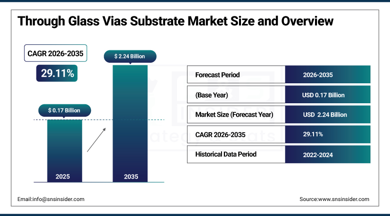
The Through Glass Vias (TGV) Substrate Market size was valued at USD 0.17 Billion in 2025 and is expected to reach USD 2.24 Billion by 2035, growing at a CAGR of 29.11% from 2026-2035.
Through glass vias substrate technology enables vertical electrical interconnections through glass, utilising high-quality borosilicate and quartz glass as base materials processed through seed layer sputtering, electroplating filling, and chemical-mechanical planarisation to achieve genuine three-dimensional interconnection. TGV technology continues gaining traction as the semiconductor industry pushes beyond the limitations of traditional silicon-based packaging, with glass substrates offering superior electrical insulation, thermal stability, and optical transparency that position the technology as a critical enabler for next-generation electronics. Rising adoption across RF components, MEMS, photonics, and increasingly high-performance computing packaging continues to widen the addressable market well beyond the technology's original niche applications. As AI and high-performance computing growth continues driving performance requirements beyond what organic substrates can support, glass substrates are increasingly viewed as the critical enabler for continued semiconductor packaging advancement.
⮞In January 2026, Intel debuted its first sample combining EMIB packaging with a glass core substrate at NEPCON Japan, achieving what the industry terms No SeWaRe, meaning no micro-cracks at panel edges during singulation, marking a decisive step toward commercial reality for glass core packaging. Intel has been an active mover in glass substrate technology since committing to the approach in its advanced packaging roadmap in 2023.
To Get more information On Through Glass Vias Substrate Market - Request Free Sample Report
Through Glass Vias (TGV) Substrate Market Trends
-
Rising adoption of laser drilling techniques enabling finer via formation for high-density interconnects.
-
Growing investment in glass core substrate pilot lines by leading semiconductor and materials manufacturers.
-
Expanding use of TGV technology across photonics and optical interconnect applications beyond RF components.
-
Increasing panel-level packaging development supporting larger format substrates beyond conventional wafer sizes.
-
Rising government semiconductor incentive investment supporting domestic advanced packaging capacity build-out.
-
Growing customer qualification activity among leading chipmakers evaluating glass substrates for AI accelerators.
U.S. Through Glass Vias (TGV) Substrate Market Outlook
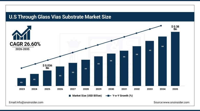
The U.S. Through Glass Vias (TGV) Substrate Market was valued at USD 0.036 Billion in 2025 and is expected to reach USD 0.38 Billion by 2035, growing at a CAGR of 26.60% from 2026-2035.
The domestic demand for such technology remains supported by the leadership of the country in terms of semiconductors innovation and high-end consumer electronics, along with the increasing deployment of 5G and AI infrastructure. Government funding programs, which include CHIPS Act funding, will continue to improve the manufacturing capacity of the country and create an ideal atmosphere for TGV technology proliferation.
⮞By 2025, Absolics, a subsidiary of South Korea's SK Group, continued deploying prototype production at its factory in Georgia with an annual production capacity of approximately 12,000 square metres, targeting completion of mass production preparation. The company produced mass-production samples during the first quarter and began customer qualification reportedly including major AI chipmakers, positioning its domestic facility as a genuine proving ground for glass substrate commercialisation.
Through Glass Vias (TGV) Substrate Market Segment Analysis
-
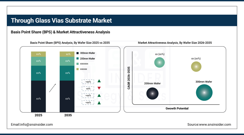
By Wafer Size, the 300mm Wafer segment dominated the market with a 52.60% share in 2025, while the Below 150mm Wafer segment is the fastest growing with a CAGR of 31.60% during 2026-2035.
-
By Application, the Consumer Electronics segment dominated the market with a 54.60% share in 2025, while the Photonics segment is the fastest growing with a CAGR of 32.60% during 2026-2035.
-
By Manufacturing Technique, the Via Etching segment dominated the market with a 48.60% share in 2025, while the Laser Drilling segment is the fastest growing with a CAGR of 33.60% during 2026-2035.
-
By End-User Industry, the Consumer Electronics Manufacturers segment dominated the market with a 46.60% share in 2025, while the Telecommunications segment is the fastest growing with a CAGR of 32.60% during 2026-2035.
By Wafer Size, 300mm Wafer Dominates the Market and Below 150mm Wafer Grows Fastest
The segment with the 300mm wafer retained market dominance in 2025. The 300mm wafer remains an attractive option for mass semiconductor packaging and MEMS production due to its scalability and precision of the via formation process; the 300mm wafer allows to integrate thousands of vias with improved uniformity and thermal dissipation capacity, as well as with significantly reduced signal interference compared to the smaller wafer sizes. In addition, the increased surface area provided by the 300mm wafer allows for cost-efficient fabrication of optical interconnects and photonic circuits, making it still a popular choice for the AI accelerators, LiDAR, and 5G transceivers production.
Below 150mm wafers are projected to be the fastest-growing wafer size category over the forecast period. Rising demand for advanced 3D packaging in smartphones and wearable devices continues to require increasingly compact substrate formats capable of supporting high-density interconnects within genuinely space-constrained device form factors. As device miniaturisation continues intensifying across consumer electronics and MEMS applications, this smaller wafer format continues to capture increasing specification activity relative to the broader, larger-wafer-dominated size mix.
⮞In December 2025, Dai Nippon Printing (DNP) announced a new TGV glass-core substrate pilot line at its Kuki Plant in Japan. The line supports 510 × 515 mm panel processing, with sample shipments planned for early 2026 and mass-production verification aimed at next-generation semiconductor packaging.
By Application, Consumer Electronics Dominates the Market and Photonics Grows Fastest
Consumer electronics dominated the market in 2025. The sheer global production volume of smartphones, wearables, and other consumer devices continues to anchor this application category as the largest source of TGV substrate demand, with billions of mobile devices shipped globally requiring high-density interconnects that TGV technology continues to enable more effectively than legacy packaging approaches. This established, high-volume manufacturing base continues to sustain consumer electronics as the clear leading application category across the broader TGV substrate market.
Photonics applications are projected to be the fastest-growing application category over the forecast period. Rising adoption of optical interconnects, LiDAR systems, and advanced photonic circuits continues to leverage glass substrates' genuine optical transparency advantage, a property that silicon-based alternatives simply cannot replicate. As data centre and autonomous vehicle applications continue driving demand for high-speed optical interconnection, photonics continues to capture an increasing share of overall TGV substrate specification activity relative to the broader, consumer-electronics-dominated application mix.
⮞In May 2026, DNP announced technical presentations on high-density polymer waveguide integration on glass substrates for co-packaged optics at the IEEE Electronic Components and Technology Conference.
By Manufacturing Technique, Via Etching Dominates the Market and Laser Drilling Grows Fastest
Via etching dominated the market in 2025. This established manufacturing technique continues to represent the most widely deployed approach for forming through-glass vias across current commercial production, benefiting from decades of accumulated process engineering refinement and a broadly established equipment and materials supply chain that continues to support reliable, repeatable via formation at production scale.
Laser drilling is projected to be the fastest-growing manufacturing technique over the forecast period. This technique continues gaining traction for finer via formation, with a meaningful and growing share of new TGV substrates across Asia Pacific specifically adopting laser drilling to achieve the tighter via geometries that increasingly demanding high-density interconnect applications require. As chip designers continue pushing toward smaller via diameters and higher via density, laser drilling continues to capture increasing manufacturing share relative to the broader, etching-dominated technique mix.
⮞In May 2025, Nippon Electric Glass announced two TGV glass-core substrate designs compatible with laser modification and etching, and CO₂ laser processing. The company began providing samples of the substrates, including 515 × 510 mm panels with TGVs formed in-house, broadening its manufacturing options for advanced semiconductor packaging.
By End-User Industry, Consumer Electronics Manufacturers Dominates the Market and Telecommunications Grows Fastest
Consumer electronics manufacturers dominated the market in 2025. These companies continue to represent the largest source of TGV substrate demand, reflecting their direct responsibility for producing the smartphones, wearables, and other consumer devices that constitute the bulk of overall global TGV substrate consumption, a scale advantage that continues to anchor this end-user category as the clear market leader.
Telecommunications is projected to be the fastest-growing end-user industry over the forecast period. Rising 5G base station deployment and antenna infrastructure buildout continues to require high-frequency, high-density interconnect solutions that TGV technology delivers effectively, as telecommunications equipment manufacturers increasingly adopt via etching and laser drilling techniques to meet the demands of high-density, high-frequency applications, positioning this end-user category for sustained above-market growth relative to the broader, consumer-electronics-dominated end-user mix.
⮞In May 2026, DNP presented work on glass-substrate integration for co-packaged optics, a technology direction relevant to high-bandwidth optical connections in advanced computing and communications systems. This is an R&D development rather than evidence of a commercial telecommunications deployment.
Regional Analysis
|
Region |
Major Country |
Share within Region, 2025 |
|---|---|---|
|
Asia Pacific |
China |
38.60% |
|
North America |
United States |
84.60% |
|
Europe |
Germany |
27.60% |
|
Latin America |
Brazil |
24.60% |
|
Middle East & Africa |
United Arab Emirates |
22.60% |
Asia Pacific Through Glass Vias (TGV) Substrate Market Insights
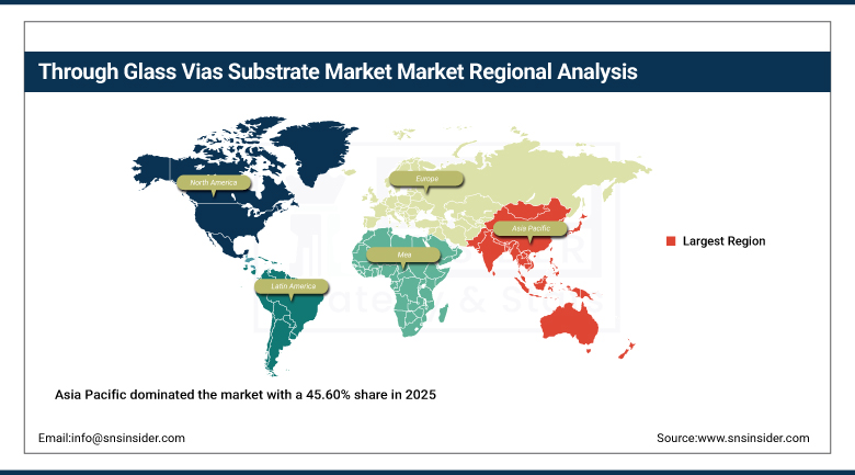
Asia Pacific dominated the market with a 45.60% share in 2025, and is also projected to grow fastest over the forecast period, registering a CAGR of approximately 30.60%. The region's extensive semiconductor manufacturing base across China, Japan, South Korea, and Taiwan continues to anchor this leadership position, reinforced by strong demand from consumer electronics, 5G infrastructure, and advanced packaging facilities concentrated across major chip-production hubs.
China's rapid expansion continues to be driven by government policies aimed at achieving semiconductor self-sufficiency, massive investments in domestic manufacturing capacity, and the rise of local device manufacturers seeking advanced packaging solutions. Japan's established glass materials expertise, exemplified by leading manufacturers scaling ceramic-reinforced glass core panels, alongside South Korea's aggressive glass substrate commercialisation efforts, continues to reinforce Asia Pacific's position as both the largest and fastest-growing regional market through the forecast period.
⮞In September 2025, China published a technical standard for through-glass via processes used in 3D semiconductor packaging. The standard covers raw-material requirements, process specifications, testing, validation, and environmental and safety requirements, reflecting progress toward more standardized TGV manufacturing practices.
Get Customized Report as per Your Business Requirement - Enquiry Now
North America Through Glass Vias (TGV) Substrate Market Insights
North America constitutes a substantial portion of the world market, given that the nation has been at the forefront of semiconductor innovations, state-of-the-art consumer electronics manufacturing and rapid adoption of 5G network infrastructure. Increased governmental spending on semiconductor R&D efforts, in line with the CHIPS Act, further strengthens its manufacturing capabilities while creating an ideal atmosphere for TGV technology commercialization.
The presence of major original equipment manufacturers and foundries investing in advanced packaging solutions continues to accelerate regional market expansion, benefiting from a well-established supply chain, cutting-edge research institutions, and a highly skilled workforce collectively enabling rapid commercialisation of innovative TGV applications. Canada contributes additional incremental regional demand as its own electronics manufacturing sector continues to develop.
Europe Through Glass Vias (TGV) Substrate Market Insights
Europe represents a meaningful share of the global market, anchored by Germany's substantial industrial and automotive electronics manufacturing base alongside the region's established glass materials science expertise, including leading raw glass suppliers headquartered within the continent.
Austria's emerging glass-core research and development activity, alongside continued investment from established European glass materials manufacturers, continues to position the region as a genuine contributor to global TGV technology advancement even as commercial-scale production capacity remains concentrated primarily within Asia Pacific and North America.
MEA & Latin America Through Glass Vias (TGV) Substrate Market Insights
The Middle East & Africa market remains comparatively modest, with growing electronics assembly and telecommunications infrastructure investment across the United Arab Emirates and Saudi Arabia gradually supporting regional interest in advanced semiconductor packaging technology as broader digital infrastructure investment continues.
Latin America's market is anchored by Brazil, where a developing domestic electronics manufacturing sector sustains gradual demand growth. Mexico contributes further incremental growth as regional electronics assembly continues to expand alongside broader nearshoring-driven manufacturing investment.
Market Dynamics
Growth Drivers: AI-Driven Packaging Demand and High-Density Interconnect Requirements
Demand for high-speed interconnects and compact device packaging stands as the primary growth driver, as the semiconductor industry continues pushing beyond the limitations of traditional silicon-based packaging toward chiplets, 2.5D and 3D-IC integration, and heterogeneous system architectures. Rising AI and high-performance computing growth continues driving performance requirements beyond organic substrate capabilities, positioning glass substrates as a critical enabler for continued semiconductor packaging advancement.
Increasing 3D integration and photonics adoption represents a second major driver, reinforced by MEMS-based miniaturisation trends across consumer electronics, automotive, and telecommunications applications. Rising wafer-level packaging adoption, AI-driven process automation, and continued defect reduction in TGV manufacturing continue to reinforce sustained market expansion as manufacturing processes mature.
⮞In December 2025, DNP announced a dedicated TGV glass-core substrate pilot line designed to address advanced packaging requirements associated with chiplet architectures and larger semiconductor packages.
Restraints: High Tooling Costs and Manufacturing Complexity
High tooling costs remain a genuine restraint, as establishing TGV substrate production capability requires substantial capital investment in specialised glass processing, via formation, and metallisation equipment that continues to limit how quickly new manufacturers can meaningfully enter this emerging technology category at commercial scale.
Processing complexity presents a further restraint, as scaling TGV formation processes for high-volume manufacturing remains a significant challenge given stringent demands for repeatability and reliability, with defect rates in early-stage production lines continuing to constrain yield and cost competitiveness relative to established organic substrate alternatives.
Opportunities: Glass Core Substrate Commercialisation and Advanced Packaging Adoption
Continued commercialisation of glass core substrates for AI accelerator packaging represents a substantial opportunity, as manufacturers that can achieve reliable, high-yield production at commercial scale stand to capture meaningful demand from chipmakers seeking to overcome the physical limitations organic substrates increasingly face in supporting next-generation AI and high-performance computing packages.
Continued expansion into photonics and high-frequency radar system applications offers a further avenue for growth, as manufacturers that can extend TGV technology's optical transparency and electrical insulation advantages into these demanding applications are positioned to capture significant new demand beyond the technology's traditional consumer electronics stronghold.
⮞In May 2025, Nippon Electric Glass began offering samples of large TGV glass-core substrates compatible with laser modification and etching or CO₂ laser processing. The development creates opportunities for semiconductor packaging customers to evaluate different via-formation approaches and glass-core designs for high-density interconnect applications.
Recent Developments:
-
2025: Dai Nippon Printing began phased operation of a TGV glass-core pilot line at its Kuki plant in Saitama, Japan, processing 510mm by 515mm panels, with sample shipments planned from early 2026 and full mass production targeted for fiscal 2028.
-
2026: Samsung Electro-Mechanics continued targeting mass production of glass core substrates between 2026 and 2027, while Samsung Electronics continued long-term development of glass interposers targeted for introduction into advanced packaging processes in 2028.
-
2026: Nippon Electric Glass scaled its ceramic-reinforced GC Core panel to a 515mm by 510mm format at 1mm thickness, expanding its glass substrate manufacturing capability for advanced packaging applications.
Through Glass Vias (TGV) Substrate Companies are
-
LPKF Laser & Electronics AG
-
Samtec, Inc.
-
KISO WAVE Co., Ltd.
-
Tecnisco Ltd.
-
Microplex GmbH
-
NSG Group
-
Allvia, Inc.
-
SCHOTT AG
-
AGC Inc.
-
Xiamen Sky Semiconductor Technology Co., Ltd.
-
Applied Materials, Inc.
-
3D Glass Solutions, Inc.
-
Absolics Inc. (SKC)
-
Nippon Electric Glass Co., Ltd.
-
Dai Nippon Printing Co., Ltd.
-
Toppan Inc.
-
Intel Corporation
-
Samsung Electro-Mechanics Co., Ltd.
Through Glass Vias (TGV) Substrate Market Report Scope:
| Report Attributes | Details |
|---|---|
| Market Size in 2025 | USD 0.17 Billion |
| Market Size by 2035 | USD 2.24 Billion |
| CAGR | CAGR of 29.11% From 2026 to 2035 |
| Base Year | 2025 |
| Forecast Period | 2026-2035 |
| Historical Data | 2022-2024 |
| Report Scope & Coverage | Market Size, Segments Analysis, Competitive Landscape, Regional Analysis, DROC & SWOT Analysis, Forecast Outlook |
| Key Segments | • By Wafer Size (300mm Wafer, 200mm Wafer, Below 150mm Wafer) • By Application (Consumer Electronics, RF Components/5G, MEMS, Photonics, Others) • By Manufacturing Technique (Laser Drilling, Via Etching, Sandblasting, Others) • By End-User Industry (Semiconductor Foundries & OEMs, Consumer Electronics Manufacturers, Automotive Electronics, Telecommunications, Others) |
| Regional Analysis/Coverage | North America (US, Canada), Europe (Germany, UK, France, Italy, Spain, Russia, Poland, Rest of Europe), Asia Pacific (China, India, Japan, South Korea, Australia, ASEAN Countries, Rest of Asia Pacific), Middle East & Africa (UAE, Saudi Arabia, Qatar, South Africa, Rest of Middle East & Africa), Latin America (Brazil, Argentina, Mexico, Colombia, Rest of Latin America). |
| Company Profiles | Corning Incorporated, LPKF Laser & Electronics AG, Samtec, Inc., KISO WAVE Co., Ltd., Tecnisco Ltd., Microplex GmbH, Plan Optik AG, NSG Group, Allvia, Inc., SCHOTT AG, AGC Inc., Xiamen Sky Semiconductor Technology Co., Ltd., Applied Materials, Inc., 3D Glass Solutions, Inc., Absolics Inc. (SKC), Nippon Electric Glass Co., Ltd., Dai Nippon Printing Co., Ltd., Toppan Inc., Intel Corporation, Samsung Electro-Mechanics Co., Ltd. |

Frequently Asked Questions
Key players include Corning Incorporated, LPKF Laser & Electronics AG, Samtec, Inc., SCHOTT AG, AGC Inc., and Absolics Inc., among other glass substrate and materials manufacturers.
Continued commercialisation of glass core substrates for AI accelerator packaging and continued expansion into photonics and high-frequency radar applications represent the primary opportunities.
Growth is primarily driven by demand for high-speed interconnects and compact device packaging, combined with increasing 3D integration and photonics adoption.
By Wafer Size, the 300mm Wafer segment dominated the market with a 52.60% share in 2025, reflecting its scalability and precision in high-volume semiconductor packaging.
Asia Pacific dominated the market with a 45.60% share in 2025, supported by the region's extensive semiconductor manufacturing base across China, Japan, South Korea, and Taiwan.
