3D IC and 2.5D IC Packaging Market Size Analysis:
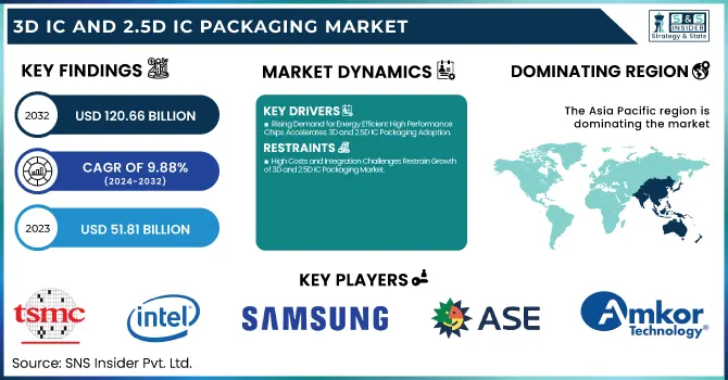
The 3D IC and 2.5D IC Packaging Market was valued at USD 51.81 billion in 2023 and is expected to reach USD 120.66 billion by 2032, growing at a CAGR of 9.88% over the forecast period 2024-2032.
To Get more information on 3D IC and 2.5D IC Packaging Market - Request Free Sample Report
The 3D IC and 2.5D IC packaging market is changing quickly towards his architecture, with modularization where a chip is designed, which can be more performant and scalable. With the advanced packaging demands, especially at the leading-edge nodes, converting and optimizing fab capacity are significantly being adjusted. High-density interconnect (HDI) PCBs are starting to become a key PCB type for 5G infrastructure to enable higher data rates and integration. At the same time, heterogeneous integration is rapidly gaining attention over monolithic methods, enabling multiple, disparate chipsets and functionalities to be combined into a single package for minimizing cost, area, power, and performance.
The U.S. 3D IC and 2.5D IC Packaging Market is estimated to be USD 11.13 Billion in 2023 and expected to reach USD 25.62 Billion by 2032 is projected to grow at a CAGR of 9.74%. The growth of the U.S. 3D IC and 2.5D IC Packaging Market is attributed to the upbeat investment in semiconductor innovation increment in computer power consumption especially driven by artificial intelligence (AI) and high-performance computers (HPC) coupled with the implementation of government initiatives including the CHIPS Act. Companies such as Intel, advancing packaging technologies, are expected to improve the performance, power efficiency, and integration density of chips.
3D IC and 2.5D IC Packaging Market Dynamics
Key Drivers:
-
Rising Demand for Energy Efficient High Performance Chips Accelerates 3D and 2.5D IC Packaging Adoption
Increasing demand for high-performance and energy-efficient semiconductor devices is one of the key factors driving the market for 3D IC and 2.5D IC packaging. Today, with fast-growing applications such as artificial intelligence (AI), high-performance computing (HPC), and 5G technology where both space and data grow immensely, the standard packaging approach is not nearly enough to provide the speed, bandwidth, and power efficiency needed. Now, the introduction of 3D ICs and 2.5D ICs provide better interconnect, higher bandwidth, smaller form factors, and thermal performance better suited for next-gen devices. In addition, dominant semiconductor players ramping up investments in heterogeneous integration and chipset-based designs are further boosting this advanced packaging technology adoption.
Restrain:
-
High Costs and Integration Challenges Restrain Growth of 3D and 2.5D IC Packaging Market
High design, development, and manufacturing costs are some of the major restraints in the 3D IC and 2.5D IC packaging market. While this is the future of semiconductor packaging, advanced packaging is much more costly than traditional packaging due to the complex equipment, unique materials, and high levels of expertise needed for 3D integration. Additionally, 3D/2.5D ICs introduce further integration challenges due to their requirement for through-silicon via (TSV) and interposer technology which compounds the cost and increases time-to-market further. However, those prices can be hard to reach, particularly for small- and medium-sized semiconductor companies or for applications where cost-effectiveness must be prioritized.
Opportunity:
-
Automotive EV and Chip Sovereignty Drive Global Demand for Robust 3D and 2.5D IC Packaging
A new one is automotive, to be especially focused on EV and autonomous driving. Detectors, radar, and AI-based processors are getting integrated into vehicles, which in turn need smaller high-volume semiconductor packages. To meet these needs, the high performance and inherent reliability of inherently robust 3D/2.5D ICs make them ideal for operation in harsh environments. Moreover, as governments worldwide are pursuing digital transfusion with ambitions of chip sovereignty, North America, Europe, and Asia Pacific regions are all experiencing an influx of backing and treasuries creating paths for regionally advanced packaging to be produced and commercialized. This results in real opportunities for existing players and start-ups along the semiconductor supply chain.
Challenges:
-
Thermal Issues Yield Loss and Design Complexity Hinder Widespread Adoption of 3D and 2.5D IC Packaging
The massive adoption still does not happen due to technical challenges of thermal management, yield issues, and design complexity. When multiple chips are stacked or placed adjacently, heat dissipation becomes even more of a challenge, especially for performance roadmaps like AI or data centers. Moreover, the testing and validation of the integrity of such small outline and multiple-layer assembly is a challenge, resulting in yield loss during manufacturing. Limited design standards, the immaturity of the ecosystem, and the lack of supply chain integration make it difficult for wider scale of these technologies and limit applications with flexible solutions.
3D IC and 2.5D IC Packaging Market Segments Analysis
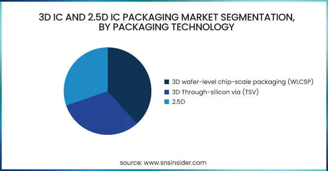
By Packaging Technology
In 2023, the 3D wafer-level chip-scale packaging (WLCSP), favored in consumer electronics, translated to a market share of 38.3%, through smartphones, tablets, and wearables. WLCSP provides a small footprint, lower packaging expense, and optimal electrical performance, making it well-suited for high-volume applications where space and cost are at a premium. It allows for direct chip mounting on printed circuit boards without the need for conventional substrates and has made it the technology of choice among manufacturers seeking miniaturization and efficiency at scale.
The 3D Through-Silicon Via (TSV) segment is expected to grow at the highest CAGR from 2024 to 2032 due to rising demand for high-bandwidth and high-performance applications. TSV allows chips to be stacked more vertically with much shorter interconnect paths that require lower energy to move data and have lower latency. It suits many high-performance applications, including advanced computing, AI, data centers, and memory, where integration density and performance are critical. With advancements in these technologies, TSV is ready for extensive integration into business verticals.
By Application
The 3D IC and 2.5D IC packaging market were led by Memory, which accounted for a hefty 34.3% share in 2023 on the back of the growing market for high-bandwidth memory (HBM), 3D NAND, and stacked DRAM. These technologies are essential for use cases where immense data transport is needed like AI, in the cloud, and advanced gaming systems. 2.5D and 3D packaging solutions provide higher density, efficiency, and lower latency with lower power delivery to facilitate next-generation memory integration for extreme data center and HPC environments.
The MEMS/Sensors segment is projected to grow at the fastest CAGR from 2024 to 2032, which is driven by the increasing demand from the automotive, healthcare, industrial automation, and consumer electronics industries. MEMS sensors need tiny and high-performance package solutions that can provide reliable and efficient MEMS sensor packaging as devices are getting smaller and smarter. Demand for advanced packaging in MEMS applications continues to increase due to trends toward IoT, smart wearables, and autonomous systems.
By End User
The 3D IC and 2.5D IC packaging market is dominated by the Consumer Electronics segment, which accounted for a 33.7% share in 2023, on account of high-volume production of smartphones, tablets, smart wearables, and AR/VR devices. Such devices require small form factors, increased performance, and low power consumption all qualities achievable through the use of 3D and 2.5D packaging technologies i.e. WLCSP and Interposer based. These packaging methods are gradually penetrating consumer devices due to the increasing high-end features, such as AI chips, high-resolution imaging, and better processors.
The Automotive industry accounted for the fastest CAGR during the forecast period of 2024 to 2032 owing to the rapid developments in electric vehicles (EVs), autonomous driving systems, and in-vehicle infotainment technologies. Such applications demand packaging solutions that are durable, reliable, and thermally efficient. The increasing use of sensors, radar, LiDAR, and AI-driven control units in today's automotive vehicles is driving automotive manufacturers to quickly adopt or deploy 3D/2.5D IC packaging.
3D IC and 2.5D IC Packaging Market Regional Insights
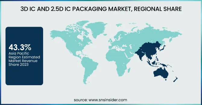
The Asia Pacific 3D IC and 2.5D IC Packaging market held the largest market share of 43.3% in 2023 and is expected to grow at the highest CAGR during the forecast period (2024-2032) due to a strong semiconductor ecosystem and aggressive technology adoption in the region. This area is the base for global semiconductor giants TSMC, Samsung Electronics, and ASE Group which almost have leading industry-level advanced packaging technology all together. Demand from consumer electronics, automotive, and AI computing drives continued investment in R&D and capital equipment by Taiwan, South Korea, Japan, and China. The regional hegemony in this area can be observed by TSMC expanding into 3D chipset integration and Samsung focusing on HBM and advanced logic packaging. Moreover, increasing government initiatives in the region such as the Made in China 2025 plan and growing investments in the developing semiconductor fabrication ecosystem in India will further consolidate Asia Pacific's high share and growth rate.
Get Customized Report as per Your Business Requirement - Enquiry Now
Key Players Listed in the 3D IC and 2.5D IC Packaging Market are:
-
TSMC (CoWoS)
-
Intel (Foveros)
-
Samsung Electronics (X-Cube)
-
ASE Group (VIPack)
-
Amkor Technology (SLIM)
-
JCET Group (3D eWLB)
-
SPIL - Siliconware Precision Industries (2.5D SiP)
-
Powertech Technology Inc. (3D TSV Packaging)
-
Micron Technology (HBM2E Memory)
-
IBM (3D TSV Integration)
-
UMC (2.5D Interposer Technology)
-
Deca Technologies (M-Series)
-
Cadence Design Systems (3D-IC Advanced Package Design Tool)
-
Synopsys (3DIC Compiler)
-
Marvell Technology (2.5D Data Center SoC)
3D IC and 2.5D IC Packaging Market Trends
-
In December 2024, TSMC's Wafer Manufacturing 2.0 revolutionized advanced packaging by integrating packaging, testing, and photomask production into core wafer fabrication.
-
In June 2024, Siemens partnered with Samsung Foundry to expand 3D-IC enablement tools and optimize EDA solutions for Samsung’s latest process nodes, boosting innovation in AI, 5G, and automotive design.
| Report Attributes | Details |
|---|---|
| Market Size in 2023 | USD 51.81 Billion |
| Market Size by 2032 | USD 120.66 Billion |
| CAGR | CAGR of 9.88% From 2024 to 2032 |
| Base Year | 2023 |
| Forecast Period | 2024-2032 |
| Historical Data | 2020-2022 |
| Report Scope & Coverage | Market Size, Segments Analysis, Competitive Landscape, Regional Analysis, DROC & SWOT Analysis, Forecast Outlook |
| Key Segments | • By Packaging Technology (3D wafer-level chip-scale packaging (WLCSP), 3D Through-silicon via (TSV), 2.5D) • By Application (Logic, Imaging & Optoelectronics, Memory, MEMS/Sensors, LED, Others) • By End User (Consumer Electronics, Industrial, Telecommunications, Automotive, Military & Aerospace, Medical Devices) |
| Regional Analysis/Coverage | North America (US, Canada, Mexico), Europe (Eastern Europe [Poland, Romania, Hungary, Turkey, Rest of Eastern Europe] Western Europe] Germany, France, UK, Italy, Spain, Netherlands, Switzerland, Austria, Rest of Western Europe]), Asia Pacific (China, India, Japan, South Korea, Vietnam, Singapore, Australia, Rest of Asia Pacific), Middle East & Africa (Middle East [UAE, Egypt, Saudi Arabia, Qatar, Rest of Middle East], Africa [Nigeria, South Africa, Rest of Africa], Latin America (Brazil, Argentina, Colombia, Rest of Latin America) |
| Company Profiles | TSMC, Intel, Samsung Electronics, ASE Group, Amkor Technology, JCET Group, SPIL, Powertech Technology Inc., Micron Technology, IBM, UMC, Deca Technologies, Cadence Design Systems, Synopsys, Marvell Technology. |
Get in Touch
