
Semiconductor Packaging Market Report Scope & Overview:
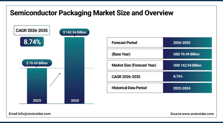
The Semiconductor Packaging Market was valued at USD 70.49 Billion in 2025 and is expected to reach USD 162.94 Billion by 2035, growing at a CAGR of 8.74% from 2026-2035.
The Semiconductor Packaging Market is growing rapidly as artificial intelligence accelerators, high-bandwidth memory, electric vehicle power modules and 5G devices shift performance gains from transistor scaling to packaging architecture. Flip chip, fan-out wafer-level, 2.5D and 3D integration allow chip designers to combine logic, memory and sensors in compact modules with shorter interconnects and lower power. Traditional leadframe and wire bond formats continue to ship in very large volumes for analog, power and microcontroller products. Foundries, memory makers and outsourced assembly and test providers are therefore investing in new plants, substrates and equipment, and the pace of capacity additions points to sustained growth through 2035. Ten-year design cycles for automotive and industrial parts add visibility to volumes.
⮞SEMI reported on 14 July 2026 that global sales of assembly and packaging equipment rose 20.8% in 2025, and projected further growth in 2026 and 2028 as advanced packaging capacity expands.
To Get More Information On Semiconductor Packaging Market - Request Free Sample Report
Semiconductor Packaging Market Trends
-
Two-and-a-half and three-dimensional packaging for artificial intelligence processors and high-bandwidth memory is driving the largest capacity investments.
-
Fan-out panel-level packaging is moving toward volume production to lower cost per package for large formats.
-
Glass and large-format organic substrates are being qualified to support bigger packages and finer interconnect pitch.
-
Heterogeneous integration through chiplets and system-in-package modules is spreading across mobile, automotive and data center chips.
-
Regional packaging plants in the United States, India, Malaysia and Vietnam are being built to diversify supply chains.
U.S. Semiconductor Packaging Market Outlook
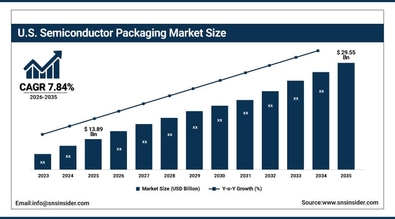
The U.S. Semiconductor Packaging Market was valued at USD 13.89 Billion in 2025 and is expected to reach USD 29.55 Billion by 2035, growing at a CAGR of 7.84% from 2026-2035.
The U.S. Semiconductor Packaging Market is the largest national market in North America, supported by leading chip designers, hyperscale data center operators, aerospace and defense contractors and a growing number of advanced packaging plants. Federal incentives are encouraging local assembly and test, which has been concentrated in Asia for decades, and new campuses in Arizona and Indiana are planned to serve artificial intelligence and memory customers. Research programs are also targeting advanced substrates and heterogeneous integration. Automotive and industrial customers demand secure local supply for power and sensor modules. These factors sustain strong growth in the U.S. through 2035. Defense programs add trusted-supply requirements.
⮞The U.S. Department of Commerce announced on 16 January 2025 USD 1.4 billion in final awards under the National Advanced Packaging Manufacturing Program, including USD 100 million for glass-core substrates.
Semiconductor Packaging Market Segment Analysis
-
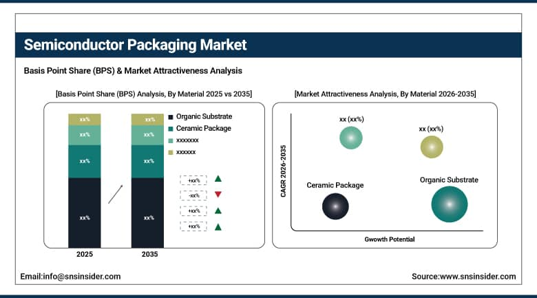
By Material, the Organic Substrate segment dominated the Semiconductor Packaging Market with approximately 41.62% share in 2025, while the Ceramic Package segment is the fastest growing with a CAGR of approximately 11.24%.
-
By Technology, the Traditional Packaging segment dominated the Semiconductor Packaging Market with approximately 51.86% share in 2025, while the Advanced Packaging segment is the fastest growing with a CAGR of approximately 11.84%.
-
By Type, the Flip Chip segment dominated the Semiconductor Packaging Market with approximately 38.74% share in 2025, while the Fan-Out WLP segment is the fastest growing with a CAGR of approximately 12.46%.
-
By End Use, the Consumer Electronics segment dominated the Semiconductor Packaging Market with approximately 43.62% share in 2025, while the Automotive segment is the fastest growing with a CAGR of approximately 11.17%.
By Material, Organic Substrate Dominates the Semiconductor Packaging Market and Ceramic Package Grows Fastest
Organic substrates lead the material segment because ball grid array, chip-scale and flip chip packages rely on laminate boards to route signals between the die and the circuit board. Suppliers in Japan, Taiwan, South Korea and Austria are expanding capacity for build-up films and large substrates that support artificial intelligence accelerators. Organic materials offer a favorable balance of cost, electrical performance and manufacturability, and their value per package is rising as layer counts and sizes increase. Bonding wire, leadframes, resins and die attach materials add recurring materials demand. Encapsulation resins, thermal interface materials and solder balls are evolving in parallel, since larger packages generate more heat and warpage, and material suppliers in Japan and Korea are launching low-stress formulations.
Ceramic packages are growing fastest as high-reliability applications expand in automotive power electronics, aerospace, medical implants, optical modules and radio frequency devices. Ceramics withstand high temperatures, provide hermetic sealing and offer stable electrical properties at high frequencies. Producers such as Kyocera are adding capacity for these parts as silicon carbide and gallium nitride devices spread. Higher unit prices and demanding qualification requirements keep volumes smaller than organic substrates, but growth rates are among the highest. Qualification of ceramic packages for silicon carbide power modules is also lengthy, so suppliers with established customer approvals hold a competitive advantage in vehicle programs.
⮞Kyocera announced on 1 September 2026 that its new plant for semiconductor packages in Isahaya, Nagasaki, was completed as part of a capital plan running through March 2029.
By Technology, Traditional Packaging Dominates the Semiconductor Packaging Market and Advanced Packaging Grows Fastest
Traditional packaging, including leadframe and wire bond formats, remains the largest technology segment by unit volume and value because analog, power, microcontroller, discrete and sensor devices still use these proven formats. Costs are low, supply chains are mature and reliability records are long, which suits automotive, industrial and consumer products. Many outsourced assembly providers run large wire bond lines in Southeast Asia and China, and customers see little reason to migrate cost-sensitive products to more complex structures. Mature nodes used in power management, automotive microcontrollers and industrial sensors keep traditional capacity full, and several outsourced providers continue to add wire bond lines in Malaysia and China.
Advanced packaging is growing fastest because artificial intelligence, high-performance computing and smartphone processors need dense interconnects and high bandwidth that cannot be achieved with traditional formats. Flip chip, system-in-package, fan-out and three-dimensional stacking allow chiplets and memory to be combined close together. Foundries and outsourced providers are investing heavily, including panel-level lines that promise lower cost for large packages. Capacity shortages for leading-edge packaging have made it a strategic priority for chip designers. Hybrid bonding, through-silicon vias and redistribution layers are the technical building blocks, and equipment suppliers report rising orders for bonders, inspection tools and plating systems.
⮞ASE's chief operating officer told shareholders in June 2026 that the company expects its first fully automated fan-out panel-level packaging line to reach mass production by the end of 2026.
By Type, Flip Chip Dominates the Semiconductor Packaging Market and Fan-Out WLP Grows Fastest
Flip chip packaging holds the largest share among advanced types because it provides short, high-density interconnects that suit processors, graphics chips, networking devices and mobile application processors. The technology is well established, with broad support from substrate makers, bumping providers and assembly houses. Variants such as flip chip ball grid array and chip-scale packages cover a wide range of price points, and the format is also the base for 2.5D interposer and chiplet products. Embedded die and system-in-package formats add specialized volume. System-in-package modules combine radio, power and processing in a single outline for earbuds, watches and sensors, and embedded die approaches place components inside the substrate to save space.
Fan-out wafer-level packaging is growing fastest as it eliminates the substrate, reduces thickness and enables heterogeneous integration of multiple dies with fine redistribution layers. Smartphone processors and power management chips use it today, and panel-level approaches are being scaled for artificial intelligence and automotive radar. Two-and-a-half and three-dimensional configurations, including interposers and hybrid bonding, are also expanding quickly. Suppliers highlight improvements in yield, warpage control and inspection as keys to wider adoption. Two-and-a-half dimensional packages using silicon or organic interposers, together with three-dimensional stacking, serve the largest artificial intelligence processors and form a distinct high-value tier.
⮞Huatian Technology disclosed on 22 May 2026 a second phase for its Nanjing advanced packaging and test base for memory chips, with 83,300 square meters of factory space and a target of 430 million chips per year.
By End Use, Consumer Electronics Dominates the Semiconductor Packaging Market and Automotive Grows Fastest
Consumer electronics accounts for the largest share because smartphones, tablets, wearables, televisions, gaming consoles and personal computers use many packaged chips per device and are produced in enormous volumes. Product refresh cycles generate consistent demand for application processors, memory, power management and connectivity chips, each requiring packaging. Premium handsets drive adoption of fan-out and system-in-package solutions, while price-sensitive devices keep volumes high for traditional formats. Industrial control, smart home and display driver devices add to volumes, and growth in wireless earbuds and smart glasses supports compact module formats with tight height limits.
Automotive is the fastest-growing end use as electrification, advanced driver assistance and software-defined vehicles increase semiconductor content per car. Power modules for inverters, radar and camera sensors, and domain controllers all need robust packages that survive heat, vibration and long lifetimes. Qualification to automotive standards lengthens development, but it creates stable, high-value demand. Healthcare, aerospace and defense, and IT and telecommunications applications add further growth through medical devices, satellites and data center networking. Healthcare devices such as hearing aids, implants and portable diagnostics need miniature, biocompatible packages, while aerospace and defense programs require radiation-tolerant and hermetic structures.
⮞The International Organization of Motor Vehicle Manufacturers reported on 23 April 2026 that global vehicle production reached 96.40 million units in 2025, with China producing 34.53 million.
Regional Analysis
|
Region |
Major Country |
Share within Region, 2025 (%) |
|---|---|---|
|
Asia Pacific |
China |
36.84% |
|
North America |
United States |
78.43% |
|
Europe |
Germany |
27.19% |
|
Latin America |
Mexico |
46.57% |
|
Middle East & Africa |
Israel |
34.62% |
Asia Pacific Semiconductor Packaging Market Insights
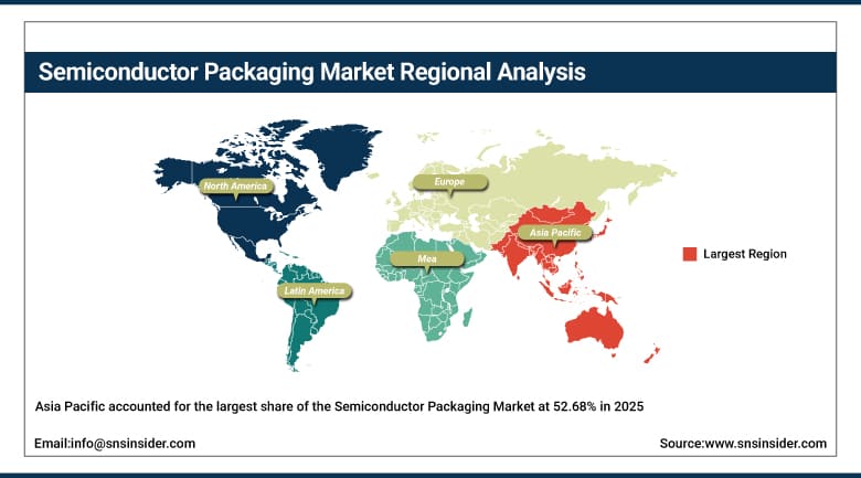
Asia Pacific accounted for the largest share of the Semiconductor Packaging Market at 52.68% in 2025, reflecting the region's dominance in outsourced assembly and test. Taiwan hosts ASE, Powertech and ChipMOS, China has JCET, Tongfu and Huatian, Malaysia, Singapore and Vietnam host plants for global chipmakers, and South Korea and Japan contribute memory and substrate leaders. TSMC's advanced packaging in Taiwan supports most leading artificial intelligence processors. Japan supplies substrates, resins and equipment through Ibiden, Shinko and Resonac, while Korea combines memory leadership with growing outsourced capacity.
Asia Pacific is also the fastest-growing region, with a CAGR of 9.72% projected for 2026-2035. Governments in India, Malaysia and Vietnam offer incentives to attract assembly and test plants, and China is expanding local capacity under self-reliance policies. High-bandwidth memory packaging in Korea and Singapore is growing quickly, and substrate makers in Japan and Taiwan are adding lines. Skilled labor, supplier clusters and proximity to electronics assembly keep the region competitive. India is moving from planning to execution with its first assembly and test plants, and Vietnam is attracting investment from memory and substrate makers.
⮞Micron broke ground on 8 January 2025 on a high-bandwidth memory advanced packaging plant in Singapore, with an investment of about USD 7 billion and operations starting in 2026.
Get Customized Report as Per Your Business Requirement - Enquiry Now
North America Semiconductor Packaging Market Insights
North America holds the second-largest share, led by the United States and supported by Canada. The region is home to leading chip designers, hyperscale cloud operators and integrated device makers such as Intel, Texas Instruments and GlobalFoundries, which operate their own packaging and assembly lines. Demand comes from artificial intelligence accelerators, networking, aerospace and defense, and medical electronics, and buyers value secure and traceable supply. Texas, Arizona, Oregon and New York host major fabs and assembly sites, and the Midwest is gaining a role in memory packaging.
Federal incentives under the CHIPS program have encouraged new packaging investments, including large campuses in Arizona and Indiana. Research consortia are developing glass substrates, hybrid bonding and chiplet standards. Dependence on Asian assembly remains high, so near-term growth is driven by pilot lines and partnerships with outsourced providers. Automotive and industrial demand in the Midwest and Texas adds volume for power and sensor modules, and growth is strong from a smaller base. Canada's contribution lies in photonics and compound semiconductor packaging, and Mexico is increasingly linked to the supply chain through assembly of electronics.
⮞Amkor announced on 8 September 2026 that phase 2 of its Arizona advanced packaging and test campus would lift its investment to about USD 12 billion on a 170-acre site.
Europe Semiconductor Packaging Market Insights
Europe is a sizable market focused on automotive, industrial and power electronics, with Germany, France, Italy and the Netherlands as principal centers. Infineon, STMicroelectronics and NXP maintain assembly and test sites, and substrate and equipment suppliers such as AT&S in Austria serve global customers. The region is strong in power module packaging for electric vehicles and renewable energy, where reliability and thermal performance are decisive. Malta, Dresden and Crolles host major fabs that feed European packaging demand, while Austria and Czechia contribute substrates and assembly.
European policy makers are working to increase local capacity and reduce dependence on imports, and pilot lines for advanced packaging are being established through research institutes in Germany, Belgium and France. Demand is tied to the automotive cycle, which has been uneven, but electrification keeps long-term volumes rising. Research centers lead in heterogeneous integration and photonics packaging. Outsourcing to Asia remains the norm for high-volume consumer products. Sweden and Finland add specialized sensor and radio packaging, and the United Kingdom focuses on compound semiconductors and design.
⮞The European Commission proposed Chips Act 2.0 on 3 June 2026, with a 12-month permitting target, and said Europe accounts for less than 10% of global chip production.
MEA & Latin America Semiconductor Packaging Market Insights
Latin America is an emerging packaging market, with Mexico, Brazil and Argentina importing most semiconductors through electronics and automotive supply chains. Mexico has the strongest potential because of its proximity to the United States and its assembly clusters, and the government has announced plans for local chip production. Brazil continues to offer tax incentives for semiconductor assembly and test, although volumes remain modest. Costa Rica is a smaller assembly and test location for medical devices and chips.
The Middle East and Africa host limited packaging capacity. Israel has a strong chip design and manufacturing base, with assembly and test activity connected to large multinational fabs, and Gulf states are exploring semiconductor strategies as part of diversification plans. Saudi Arabia and the United Arab Emirates are evaluating partnerships with global suppliers. Most demand in the sub-region is met through imports, but investments in data centers are creating new needs. Regional distributors remain important.
⮞Mexico's Economy Secretary Marcelo Ebrard said on 10 February 2026 that the country will begin producing chips by the end of 2026 at a plant under construction in Queretaro.
Market Dynamics
Growth Drivers: Artificial Intelligence Accelerators and Vehicle Electrification Drive Growth in the Semiconductor Packaging Market
Artificial intelligence accelerators are the principal growth driver because their performance depends on packaging that places logic and high-bandwidth memory side by side with very short, dense connections. Each new generation uses larger interposers, more memory stacks and greater power, so packaging value per processor increases sharply. Cloud providers and chip designers are securing capacity years ahead, encouraging foundries and assembly providers to expand lines. Telecommunications operators are also upgrading networks, and base stations, optical modules and edge servers require packaged radio and processing chips.
Vehicle electrification is a second driver. Electric vehicles carry more chips for power conversion, battery management and driver assistance, and their power modules require specialized packages with advanced thermal and electrical performance. Policies supporting electric vehicle adoption in China, Europe and India sustain demand. Rising numbers of connected devices and 5G infrastructure add further packaged chips. Hyperscale data center construction continues to expand, creating steady orders for server processors, networking silicon and memory modules. Data center spending cycles remain the largest swing factor.
⮞The International Energy Agency reported on 20 May 2026 that global electric car sales exceeded 20 million in 2025, up about 20%.
Restraints: Capital Intensity and Substrate Constraints Restrain Growth in the Semiconductor Packaging Market
Advanced packaging lines require substantial capital for bumping, bonding, inspection and cleanroom space, and returns depend on customer commitments. Smaller assembly providers may struggle to finance upgrades, which leads to concentration among a few large companies. Equipment lead times and skilled labor shortages can delay capacity additions. Environmental regulations on chemicals and water use add compliance costs for plating and etching steps, and local permitting delays can slow new plants. Smaller regional players often depend on equipment financing and long-term supply contracts to justify investment.
Shortages of high-end substrates and specialty materials have limited output in recent years, since large artificial intelligence packages need advanced build-up films and many layers. Suppliers are investing, but new capacity takes years to qualify. Yield losses on large packages, thermal management challenges and geopolitical export controls add further risk. Cyclical swings in consumer electronics can leave traditional lines underused. Currency swings, tariffs and trade restrictions on equipment and materials complicate procurement and may change the economics of regional sites.
⮞Samsung Electro-Mechanics announced on 28 September 2026 a 4.27 trillion won investment, about USD 3.14 billion, in its Sejong plant for flip chip ball grid array substrates, with mass production planned for September 2028.
Opportunities: Regional Assembly Hubs and Glass Substrates Create Opportunities in the Semiconductor Packaging Market
Government programs in India, Malaysia, Vietnam and the United States are creating regional assembly hubs, giving outsourced providers and equipment suppliers new customers and incentives. Chip designers want supply chain diversity, so plants outside Taiwan and China win qualification for strategic products. Local supplier ecosystems for materials, test and logistics can develop around these hubs. Government grants, tax credits and subsidized land lower the cost of entering new locations, and downstream customers often sign long-term supply agreements to anchor investments.
Glass substrates and panel-level processing form a second opportunity. Glass offers flatness and fine interconnect pitch that suit large artificial intelligence packages, and early pilot lines have received public funding. Co-packaged optics, silicon photonics and chiplet standards open further segments for packaging innovation. Suppliers able to combine design services, materials and test capability can capture higher-margin business. Design houses and universities near these hubs also supply talent and applied research that support yield improvement and new package concepts. Such clusters also shorten delivery times.
⮞CG Semi began commercial production at its outsourced assembly and test facility in Sanand, India in July 2026, one of 12 projects approved under the India Semiconductor Mission.
Recent Developments:
- 2025: Texas Instruments opened a second assembly and test plant in Melaka, Malaysia, with planned investment of up to MYR 5 billion over time. The six-level facility of more than 900,000 square feet handles bump, probe, assembly and test, supporting the company's goal to complete 90% of assembly and test in-house by 2030.
- 2026: Chipbond officially opened its Penang plant in Batu Kawan, Malaysia, an investment of about USD 200 million for wafer bumping, wafer-level chip-scale packaging and test. Initial capacity is 10,000 wafers and 100 million chip-scale packages per month, with customer qualification starting in the first quarter of 2026.
- 2026: Ibiden announced the second phase of its capital plan for IC package substrates for artificial intelligence servers, concentrated at its Ohno plant. Upgraded facilities are scheduled to come online in stages from fiscal 2027, adding capacity for large substrates.
- 2026: SK hynix broke ground on a high-bandwidth memory packaging and test plant in West Lafayette, Indiana, with more than USD 4 billion planned on about 133 acres. The first cleanroom is targeted for October 2028 and mass production for the second half of 2029, supporting about 1,000 direct jobs.
Semiconductor Packaging Market Key Players are:
-
ASE Technology Holding Co., Ltd.
-
Amkor Technology, Inc.
-
JCET Group Co., Ltd.
-
Tongfu Microelectronics Co., Ltd.
-
Tianshui Huatian Technology Co., Ltd.
-
Powertech Technology Inc.
-
ChipMOS Technologies Inc.
-
Chipbond Technology Corporation
-
UTAC Holdings Ltd.
-
Unisem (M) Berhad
-
Sigurd Microelectronics Corporation
-
Taiwan Semiconductor Manufacturing Company (TSMC)
-
Intel Corporation
-
Samsung Electronics Co., Ltd.
-
SK hynix Inc.
-
GlobalFoundries Inc.
-
Texas Instruments Incorporated
-
Kyocera Corporation
Semiconductor Packaging Market Report Scope:
| Report Attributes | Details |
|---|---|
| Market Size in 2025 | USD 70.49 Billion |
| Market Size by 2035 | USD 162.94 Billion |
| CAGR | CAGR of 8.74% From 2026 to 2035 |
| Base Year | 2025 |
| Forecast Period | 2026-2035 |
| Historical Data | 2022-2024 |
| Report Scope & Coverage | Market Size, Segments Analysis, Competitive Landscape, Regional Analysis, DROC & SWOT Analysis, Forecast Outlook |
| Key Segments | • By Material (Organic Substrate, Bonding Wire, Leadframes, Encapsulation Resins, Ceramic Package, Die Attach Material, and Others) • By Technology (Traditional Packaging and Advanced Packaging) • By Type (Flip Chip, System-in-Package, 2.5D/3D, Embedded Die, Fan-In WLP, and Fan-Out WLP) • By End Use (Consumer Electronics, Automotive, Healthcare, IT and Telecommunication, Aerospace and Defense, and Others) |
| Regional Analysis/Coverage | North America (US, Canada), Europe (Germany, UK, France, Italy, Spain, Russia, Poland, Rest of Europe), Asia Pacific (China, India, Japan, South Korea, Australia, ASEAN Countries, Rest of Asia Pacific), Middle East & Africa (UAE, Saudi Arabia, Qatar, South Africa, Rest of Middle East & Africa), Latin America (Brazil, Argentina, Mexico, Colombia, Rest of Latin America). |
| Company Profiles | ASE Technology Holding Co., Ltd., Amkor Technology, Inc., JCET Group Co., Ltd., Tongfu Microelectronics Co., Ltd., Tianshui Huatian Technology Co., Ltd., Powertech Technology Inc., ChipMOS Technologies Inc., Chipbond Technology Corporation, UTAC Holdings Ltd., Unisem (M) Berhad, Sigurd Microelectronics Corporation, Taiwan Semiconductor Manufacturing Company (TSMC), Intel Corporation, Samsung Electronics Co., Ltd., SK hynix Inc., GlobalFoundries Inc., Texas Instruments Incorporated, Kyocera Corporation |

Frequently Asked Questions
The key players in the Semiconductor Packaging Market include ASE Technology Holding Co., Ltd., Amkor Technology, Inc., JCET Group Co., Ltd., Tongfu Microelectronics Co., Ltd., Taiwan Semiconductor Manufacturing Company, among others.
Key opportunities include regional assembly hubs in India, Malaysia, Vietnam and the United States, glass substrates and panel-level processing, and co-packaged optics.
The major growth factor is demand for advanced packaging by artificial intelligence accelerators and high-bandwidth memory, together with vehicle electrification.
The Traditional Packaging segment dominated the Semiconductor Packaging Market with approximately 51.86% share in 2025, supported by large volumes of analog, power and microcontroller devices.
Asia Pacific dominated the Semiconductor Packaging Market with a 52.68% share in 2025, driven by outsourced assembly and test capacity in Taiwan, China, South Korea and Southeast Asia.
