FinFET Technology Market Report Scope & Overview:
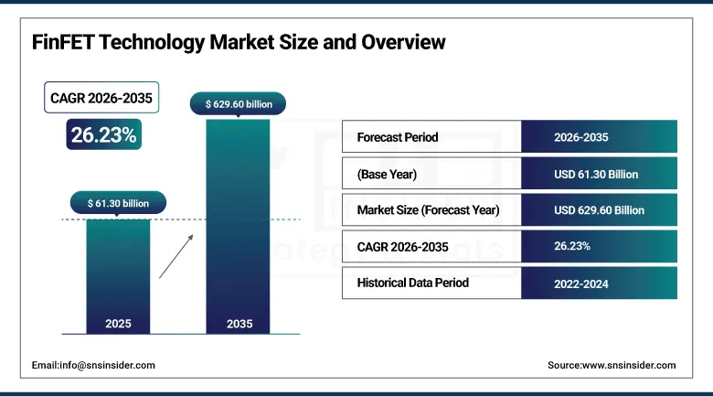
The FinFET Technology Market was valued at USD 61.30 billion in 2025 and is expected to reach USD 629.60 billion by 2035, growing at a CAGR of 26.23% from 2026–2035.
The global FinFET (Fin Field-Effect Transistor) technology market is at the centre of the semiconductor industry's most consequential technology transition in a generation, as the three-dimensional multi-gate transistor architecture that replaced planar transistors at the 22nm node has become the definitive enabling technology for every major semiconductor process node below 14nm, including 10nm, 7nm, 5nm, 3nm, and the emerging sub-2nm nodes defining the frontier of computing performance and power efficiency through the forecast period. FinFET technology's three-dimensional gate-over-fin structure provides superior electrostatic control of the transistor channel, suppressing the leakage current that rendered planar transistors impractically inefficient below 22nm, while simultaneously delivering higher switching speed and lower operating voltage that enable each new process generation to deliver the power-performance improvements driving semiconductor application value. The technology is the foundational architecture enabling the AI computing revolution, as the extraordinary processing density and energy efficiency of modern AI accelerator chips implemented in 5nm and 3nm FinFET processes make the training and inference of large language models commercially viable at server scale. Every major semiconductor foundry including TSMC, Samsung Foundry, Intel Foundry, and GlobalFoundries relies on FinFET-based processes as the cornerstone of their advanced node product portfolios.
The FinFET Technology Market's extraordinary 26.23% CAGR from 2026 to 2035 reflects the structural lock-in of FinFET architecture across every high-performance semiconductor application from smartphone SoCs and AI accelerators through automotive safety processors and 5G base station chips, where there is no commercially viable alternative technology at process nodes below 14nm. The semiconductor industry's insatiable demand for more processing capability at lower power consumption per transistor operation, driven by AI, 5G, autonomous vehicles, and edge computing, creates a compounding demand flywheel sustaining FinFET's exceptional market growth through the entire forecast horizon.
FinFET Technology Market Size and Forecast
-
Market Size in 2025: USD 61.30 Billion
-
Market Size by 2035: USD 629.60 Billion
-
CAGR: 26.23% from 2026 to 2035
-
Base Year: 2025
-
Forecast Period: 2026–2035
-
Historical Data: 2022–2024
To Get more information on FinFET Technology Market - Request Free Sample Report
FinFET Technology Market Trends
-
Accelerating transition to 5nm and 3nm FinFET process nodes driven by the AI semiconductor industry's demand for maximum transistor density and minimum power consumption per AI operation, enabling increasingly powerful large language model inference capability within server power budgets that data centres can practically provision.
-
Growing adoption of FinFET technology in automotive safety processors as ISO 26262 functional safety requirements drive automotive semiconductor manufacturers to adopt advanced process nodes delivering the processing performance required for ADAS sensor fusion and autonomous driving decision-making within stringent automotive operating environment specifications.
-
Rapid expansion of FinFET-based custom silicon programmes at hyperscale cloud operators including Google (TPU), Amazon (Trainium and Inferentia), and Microsoft (Maia), where proprietary AI accelerator chip development using TSMC's advanced FinFET processes creates growing fabless design volumes expanding the market's addressable revenue base.
-
Increasing development and commercialisation of nanosheet transistor architecture, also known as gate-all-around, as the next evolutionary step beyond FinFET at sub-3nm nodes, with Samsung's 3nm GAA deployment and TSMC's planned N2 process transition representing the technology progression succeeding FinFET at the frontier of process node scaling.
-
Growing demand for FinFET-based RISC-V processor implementations as the open-source instruction set architecture enables new market participants to design competitive computing products without ARM or x86 licence fees, expanding the community of designers implementing silicon on advanced FinFET process nodes.
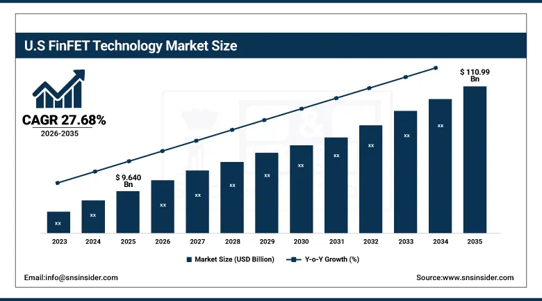
U.S. FinFET Technology Market was valued at USD 9.640 billion in 2025 and is expected to reach USD 110.99 billion by 2035, growing at a CAGR of 27.68% during 2026–2035.
The United States represents the world's most commercially dynamic FinFET technology market, anchored by the world's leading fabless semiconductor design companies including NVIDIA, AMD, Qualcomm, Apple, and Intel whose continuous product innovation cycles create the largest single-country demand for advanced FinFET process node foundry capacity. The CHIPS and Science Act's USD 52 billion domestic semiconductor manufacturing investment programme is catalysing TSMC, Samsung, Intel, and Micron to establish or expand advanced FinFET manufacturing in the United States. U.S. AI chip demand is the most powerful single demand driver in the global FinFET market, as NVIDIA's AI GPU production volumes at TSMC's 5nm and 4nm nodes represent one of the largest single-customer advanced process node consumption profiles in the history of the semiconductor industry.
FinFET Technology Market Segment Insights
-
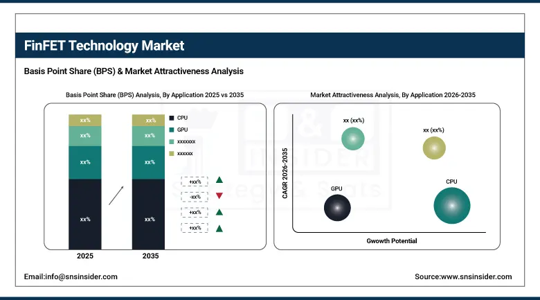
According to Application, CPU dominated with approximately 29% market share in 2024; GPU is the fastest-growing application at approximately 30.26% CAGR from 2026 to 2035 driven by AI training and gaming workload demand.
-
In terms of Node Size, 14nm dominated with approximately 19% market share in 2024 as the most broadly deployed high-volume FinFET node; 5nm is the fastest-growing node at approximately 30.99% CAGR driven by AI accelerator and premium smartphone SoC adoption.
-
By End-Use Industry, Consumer Electronics dominated in 2024 as the largest semiconductor application segment; Automotive is one of the fastest-growing end-use verticals driven by ADAS processor adoption and ISO 26262 functional safety requirements.
FinFET Technology Market Segment Analysis
By Application: CPU dominates, GPU grows fastest
The CPU application segment dominated the FinFET Technology Market in 2024 with approximately 29% of revenues, driven by the continuous global demand for high-performance central processing units in personal computers, servers, workstations, and embedded computing systems that represent the most broadly deployed semiconductor application requiring advanced FinFET process nodes. CPUs from Intel, AMD, Apple, Qualcomm, and ARM-based processor designers collectively consume enormous volumes of advanced FinFET process capacity across TSMC, Samsung, and Intel Foundry facilities. The data centre server CPU market is a particularly significant FinFET demand driver, as the cloud computing industry's continuous capacity expansion across AWS, Azure, Google Cloud, and domestic data centre operators sustains predictable, large-volume advanced node CPU procurement that constitutes one of the most commercially reliable FinFET revenue streams in the market.
The GPU application segment is projected to grow at the fastest CAGR of approximately 30.26% from 2026 to 2035, driven by the extraordinary growth of AI computing workloads that have transformed GPU from a graphics rendering component into the primary compute engine for training and inference of large language models, computer vision systems, and recommendation algorithms across the global AI infrastructure buildout. NVIDIA's dominant GPU architecture, implemented on TSMC's most advanced FinFET process nodes, represents the most concentrated single-application demand driver for cutting-edge FinFET process technology in the semiconductor industry. As AI model complexity grows and inference deployment scales from data centres to edge devices, GPU FinFET volumes are expected to expand at an exceptional rate through the forecast period.
By Node Size: 14nm dominates, 5nm grows fastest
The 14nm node retained the largest segment share of approximately 19% of the FinFET Technology Market in 2024, reflecting its status as the most broadly deployed advanced FinFET process node across the highest-volume semiconductor applications. 14nm FinFET technology, commercially introduced simultaneously by Intel, Samsung, and TSMC between 2014 and 2015, has been in volume production for over a decade and benefits from mature manufacturing yield, broad supplier ecosystem support, and the widest design rule library availability of any advanced FinFET node. Its performance and power efficiency are well-matched to a wide range of mid-range consumer electronics, industrial microcontrollers, automotive processors, and communications infrastructure applications where the cost premiums of sub-10nm nodes are not commercially justified.
The 5nm node is projected to grow at the fastest CAGR of approximately 30.99% through 2035, driven by adoption in the most performance-demanding AI accelerators, premium smartphone SoCs, and next-generation server processors where each additional transistor density improvement at 5nm translates directly into commercially significant AI model throughput, battery life, or thermal envelope improvements. Apple's A-series processors, NVIDIA's H-series AI GPUs, and AMD's Zen 4 CPUs are all implemented on TSMC's 5nm family process generations, establishing 5nm as the premier high-volume advanced node generating the highest per-wafer revenue in TSMC's production portfolio and sustaining exceptional growth in the most technically and commercially demanding FinFET semiconductor applications.
By End-Use Industry: Consumer Electronics dominates, Automotive grows fastest
Consumer Electronics dominated the FinFET Technology end-use segmentation across the forecast period as the largest semiconductor application category consuming advanced FinFET process capacity, driven by the smartphone market's annual consumption of hundreds of millions of advanced SoC units and the equally large volumes of tablets, laptops, smart TVs, wearables, and gaming consoles each requiring FinFET-based processors. Smartphone SoC design has consistently driven the leading edge of FinFET process node commercialisation, with Apple, Qualcomm, and MediaTek SoC designs providing the volume anchor justifying TSMC and Samsung's investment in each new process generation. The consumer electronics sector's product replacement cycle creates predictable, high-volume, time-bounded demand for advanced FinFET process capacity that sustains the financial model underlying foundry investment in cutting-edge FinFET nodes.
Automotive is one of the fastest-growing end-use verticals for FinFET technology, as the automotive industry's requirements for ADAS sensor fusion, autonomous driving decision processors, and EV power management systems are driving OEM specifications for automotive-grade semiconductor solutions implemented on advanced FinFET process nodes. The automotive sector's long product qualification cycles and AEC-Q100 automotive reliability certification requirements have historically led automotive semiconductor adoption of advanced process nodes, but the urgent commercial pressure of autonomous vehicle and EV programme timelines is compressing qualification periods and driving rapid automotive FinFET adoption through the forecast period.
FinFET Technology Market Regional Analysis
|
Region |
Major Country |
Share within Region (%) |
|---|---|---|
|
North America |
United States |
~85% |
|
Europe |
Germany |
~32% |
|
Asia Pacific |
Taiwan |
~52% |
|
Middle East & Africa |
Israel |
~34% |
|
Latin America |
Brazil |
~42% |
Asia Pacific FinFET Technology Market Insights
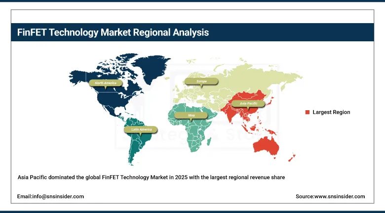
Asia Pacific dominated the global FinFET Technology Market in 2025 with the largest regional revenue share, anchored by Taiwan's extraordinary TSMC foundry operations manufacturing the majority of the world's most advanced FinFET semiconductor devices including Apple, NVIDIA, AMD, and Qualcomm products, combined with South Korea's Samsung Electronics and SK Hynix advanced semiconductor operations, Japan's semiconductor materials and equipment leadership, and China's rapidly growing domestic fabless design industry. Taiwan's TSMC represents the most commercially critical FinFET manufacturing asset in the global technology supply chain.
Get Customized Report as per Your Business Requirement - Enquiry Now
North America FinFET Technology Market Insights
North America is projected to register the fastest regional CAGR of 29.44% through 2035, driven by the extraordinary commercial momentum of U.S.-based AI semiconductor design companies including NVIDIA, AMD, Apple, Qualcomm, and Broadcom whose continuous product innovation cycles at advanced FinFET nodes are the primary demand driver for the world's most advanced semiconductor manufacturing capacity. The CHIPS and Science Act's domestic manufacturing investment programme is adding TSMC Arizona N3 and N2 advanced node capacity, Samsung Taylor Texas facility, and Intel Ohio fab capacity that will increase U.S.-soil FinFET manufacturing capability significantly through the forecast period.
Europe FinFET Technology Market Insights
Europe is a growing FinFET technology market anchored by automotive semiconductor demand from German, French, and Italian OEM customers specifying advanced FinFET-based safety processors for ADAS and autonomous driving applications, combined with telecommunications infrastructure semiconductor procurement and the European Chips Act's EUR 43 billion semiconductor investment commitment supporting TSMC Dresden, Intel Magdeburg, and domestic European foundry development.
Latin America and MEA FinFET Technology Market Insights
Latin America and MEA are growing FinFET technology consumers, driven primarily by semiconductor-intensive telecommunications infrastructure investment, consumer electronics market growth, and nascent automotive electronics adoption. Israel is the leading MEA market participant through its world-class semiconductor design industry encompassing Intel's design centre, Tower Semiconductor, and multiple AI chip startup companies developing specialised FinFET-based AI inference accelerators. Brazil leads Latin American FinFET market revenues through its large electronics consumer market and growing telecommunications infrastructure programme.
FinFET Technology Market Growth Drivers:
-
AI computing infrastructure buildout fundamentally requiring advanced FinFET nodes to achieve the transistor density and power efficiency enabling commercial-scale AI deployment
The primary structural growth driver for the FinFET Technology Market is the extraordinary and accelerating investment in AI computing infrastructure that fundamentally requires advanced FinFET semiconductor technology to achieve the processing capability and energy efficiency targets making large-scale AI commercially and operationally viable. NVIDIA's AI GPU products implemented on TSMC's most advanced FinFET nodes are the most commercially significant single product family in the semiconductor industry by revenue, and the AI infrastructure buildout programmes of major cloud operators committing hundreds of billions of dollars to data centre construction are directly translating into semiconductor procurement programmes overwhelmingly relying on advanced FinFET process capacity for AI training and inference accelerator production.
The proliferation of FinFET-based custom AI accelerator programmes at Amazon, Google, Microsoft, and Meta, combined with the rapid growth of AI chip startup companies designing specialised FinFET inference accelerators for edge and data centre deployment, represents a fundamental broadening of the advanced FinFET customer base beyond the traditional CPU and GPU market that will sustain demand growth well beyond the lifecycle of any individual product generation through the 2026 to 2035 forecast period.
FinFET Technology Market Restraints
-
Extreme manufacturing complexity and capital cost, geopolitical supply chain concentration risk in Taiwan, and design cost escalation at advanced nodes limiting market participant diversity
A significant restraint on the FinFET Technology Market is the extraordinary capital cost and manufacturing complexity of advanced FinFET foundry operations, where a new leading-edge semiconductor fabrication facility requires capital investment of USD 15 to 20 billion and two to three years of construction and tool qualification before production volumes can ramp. This barrier to entry concentrates advanced FinFET manufacturing among a very small number of global foundries, creating supply concentration risk surrounding TSMC's dominant share of the world's most advanced FinFET capacity in Taiwan. The rapidly escalating cost of advanced node chip design, where a 5nm SoC design programme can cost USD 500 million to USD 1 billion, restricts participation in leading-edge FinFET design to companies with very large addressable market opportunities and substantial R&D budgets.
FinFET Technology Market Opportunities
-
CHIPS Act domestic manufacturing expansion, edge AI inference chip proliferation, and automotive ADAS processor design adoption at advanced nodes
The CHIPS and Science Act's USD 52 billion domestic semiconductor investment programme, combined with equivalent programmes in Europe, Japan, South Korea, and India, is creating the most significant geographic diversification of FinFET manufacturing capacity in the technology's history, expanding the addressable market for FinFET wafer production beyond the current TSMC-dominated structure toward a multi-foundry, multi-geography model sustaining market revenue growth through construction, equipment procurement, and process qualification investment. Edge AI inference chip proliferation, where billions of autonomous vehicles, industrial robots, smart cameras, and AI wearables will require locally processed AI inference capability implemented on power-efficient FinFET process nodes, represents a massive volume semiconductor market only beginning to scale during the forecast period. Automotive ADAS processor adoption at advanced FinFET nodes, driven by Level 3 and Level 4 autonomous driving computational requirements, creates premium-priced, long-lifecycle design win opportunities for semiconductor companies positioning FinFET products for automotive safety qualification.
Recent Developments:
-
2025: TSMC commenced production ramp of its N3E (3nm) process at its Taiwan Fab 18 facility, delivering the world's most advanced commercially available FinFET technology with approximately 60% improvement in logic density relative to N5, serving Apple, NVIDIA, and AMD advanced product programmes.
-
2025: Intel commenced volume production at its Intel 18A process node incorporating RibbonFET and PowerVia backside power delivery, establishing Intel's return to process node leadership with a technology architecture extending FinFET performance principles into the angstrom era.
-
2025: Samsung Electronics advanced mass production qualification of its 2nm GAA process at its Taylor, Texas fab under construction, with customer product tape-outs planned for 2026 enabling advanced node semiconductor production on U.S. soil.
-
2024: NVIDIA unveiled the Blackwell B100 AI GPU architecture implemented on TSMC's custom 4NP FinFET process, delivering 2.5 times the training performance and 5 times the inference throughput of the prior Hopper generation.
-
2025: AMD launched its EPYC Turin server CPU implementing Zen 5 cores on TSMC's 3nm FinFET process, delivering the highest x86 server CPU performance in history and representing the latest generation of FinFET-enabled performance leadership in enterprise data centre computing.
FinFET Technology Market Key Players
-
Taiwan Semiconductor Manufacturing Company Ltd. (TSMC)
-
Samsung Electronics Co. Ltd.
-
Intel Corporation
-
GlobalFoundries Inc.
-
United Microelectronics Corporation (UMC)
-
NVIDIA Corporation
-
Advanced Micro Devices Inc. (AMD)
-
Qualcomm Technologies Inc.
-
Apple Inc.
-
Broadcom Inc.
-
MediaTek Inc.
-
ARM Holdings plc
-
ASML Holding N.V.
-
Cadence Design Systems Inc.
-
Synopsys Inc.
-
Marvell Technology Inc.
-
Microchip Technology Inc.
-
NXP Semiconductors N.V.
-
Renesas Electronics Corporation
-
STMicroelectronics N.V.
FinFET Technology Market Report Scope:
| Report Attributes | Details |
|---|---|
| Market Size in 2025 | USD 61.30 Billion |
| Market Size by 2035 | USD 629.60 Billion |
| CAGR | CAGR of 26.23% From 2026 to 2035 |
| Base Year | 2025 |
| Forecast Period | 2026-2035 |
| Historical Data | 2022-2024 |
| Report Scope & Coverage | Market Size, Segments Analysis, Competitive Landscape, Regional Analysis, DROC & SWOT Analysis, Forecast Outlook |
| Key Segments | • By Application (CPU, GPU, Memory, FPGA, Network Processors, MCU, Others) • By Node Size (Below 5nm, 5nm, 7nm, 10nm, 14nm, Others) • By End-Use Industry (Consumer Electronics, Data Centers and IT Infrastructure, Automotive, Telecommunications, Industrial Automation, Healthcare, Others) |
| Regional Analysis/Coverage | North America (US, Canada, Mexico), Europe (Eastern Europe [Poland, Romania, Hungary, Turkey, Rest of Eastern Europe] Western Europe] Germany, France, UK, Italy, Spain, Netherlands, Switzerland, Austria, Rest of Western Europe]), Asia Pacific (China, India, Japan, South Korea, Vietnam, Singapore, Australia, Rest of Asia Pacific), Middle East & Africa (Middle East [UAE, Egypt, Saudi Arabia, Qatar, Rest of Middle East], Africa [Nigeria, South Africa, Rest of Africa], Latin America (Brazil, Argentina, Colombia, Rest of Latin America) |
| Company Profiles | Taiwan Semiconductor Manufacturing Company Ltd. (TSMC), Samsung Electronics Co. Ltd., Intel Corporation, GlobalFoundries Inc., United Microelectronics Corporation (UMC), NVIDIA Corporation, Advanced Micro Devices Inc. (AMD), Qualcomm Technologies Inc., Apple Inc., Broadcom Inc., MediaTek Inc., ARM Holdings plc, ASML Holding N.V., Cadence Design Systems Inc., Synopsys Inc., Marvell Technology Inc., Microchip Technology Inc., NXP Semiconductors N.V., Renesas Electronics Corporation, STMicroelectronics N.V. |
Frequently Asked Questions
Ans: Asia Pacific dominated with the largest regional revenues in 2025, anchored by Taiwan's TSMC which manufactures the majority of the world's most advanced FinFET semiconductor devices for Apple, NVIDIA, AMD, and Qualcomm, combined with South Korea's Samsung Electronics advanced semiconductor operations and Japan's semiconductor materials and equipment ecosystem leadership.
Ans: The 5nm node segment is projected to grow at the fastest CAGR of approximately 30.99% through 2035, driven by adoption in the most performance-demanding AI accelerators, premium smartphone SoCs, and next-generation server processors where each transistor density improvement at 5nm translates directly into commercially significant AI throughput, battery life, or thermal envelope improvements.
Ans: The extraordinary investment in AI computing infrastructure fundamentally requiring advanced FinFET semiconductor technology to achieve the transistor density and power efficiency enabling commercial-scale AI deployment, combined with smartphone SoC demand sustaining high-volume advanced node FinFET production, and expanding automotive ADAS and EV processor adoption of FinFET-based safety semiconductors.
Ans: The FinFET Technology Market was valued at USD 61.30 billion in 2025.
Ans: The FinFET Technology Market is expected to grow at a CAGR of 26.23% from 2026 to 2035.
Get in Touch
