Nanoimprint Lithography Systems Market Report Scope & Overview:
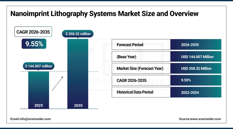
The Nanoimprint Lithography Systems Market size was valued at USD 144.007 Million in 2025 and is projected to reach USD 358.32 Million by 2035, growing at a CAGR of 9.55% during 2026–2035.
The Nanoimprint Lithography (NIL) Systems market are growing with a steady pace due to its application in high resolution and economical semiconductor manufacturing solutions NIL is a direct nanoscale pattern transfer technology based on mechanical imprinting which can serve as a more cost-effective and less complicated method for nanoscale patterning compared to the traditional optical lithography. It has applications in advanced semiconductors, photonics, memory devices, and nanostructured components. Adoption is also being further supported by the continuing trend of device miniaturization, next-generation chip architectures and advanced packaging. Higher throughput, precision, and process control are also making it increasingly relevant for industries, with NIL systems emerging as a key enabler technology in the global SOI semiconductor ecosystem.
In Sept 2024 — Canon Inc. shipped FPA-1200NZ2C nanoimprint lithography system to the Texas Institute for Electronics, specializing in NIL-based chip fabrication for semiconductor R&D, and prototype manufacturing.
Market Size and Growth:
-
Market Size in 2025: USD 144.007 Million
-
Market Size by 2035: USD 358.32 Million
-
CAGR: 9.55% (from 2026 to 2035)
-
Base Year: 2025
-
Forecast Period: 2026–2035
-
Historical Data: 2022–2024
To Get more information on Nanoimprint Lithography Systems Market - Request Free Sample Report
Nanoimprint Lithography Systems Market Trends Highlights:
-
High-resolution patterning is in strong demand due to semiconductor miniaturization and nanoscale fabrication needs
-
Semiconductor manufacturing is rapidly adopting NIL for memory devices, photonics, and advanced chips
-
NIL is a cost-effective alternative to EUV lithography with lower capital cost and high precision
-
Strong R&D is improving throughput, defect control, and scalability
-
Asia-Pacific leads the market due to strong semiconductor hubs in China, Japan, South Korea, and Taiwan
-
Applications are expanding beyond semiconductors into biotechnology, optics, and advanced displays
U.S. Nanoimprint Lithography (NIL) Systems Market Size Outlook:
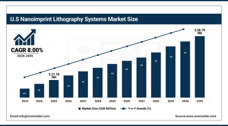
The U.S. Nanoimprint Lithography (NIL) Systems Market was valued at USD 27.18 Million in 2025 and is projected to reach USD 58.70 Million by 2035, growing at a CAGR of 8.00% during 2026–2035, influenced by rising adoption of NIL systems in photonics, memory devices, advanced packaging, and research-centric semiconductor fabrication. Another key reason for the growth of this technology in the U.S. is the technology transferring high-resolution patterns at a lower cost compared to conventional photolithography. Additionally, there is increasing collaboration between semiconductor equipment manufacturer and research institutions that is expanding capabilities for NIL process technology and improving throughput, precision and defect control over NIL process steps. Nevertheless, ongoing complexity in the process, relative immaturity in mass production, and extreme sensitivity to technical variation remain barriers to wider commercialization.
Market Drivers: Rising Demand for High-Resolution and Cost-Efficient Semiconductor Patterning Drives Nanoimprint Lithography Systems Growth
Nanoimprint Lithography Key Driving Markets Increasing demand for high-resolution, low-cost and scalable semiconductor patterning is a major market driver of NILsystems. Direct nanoscale pattern transfer with NIL through mechanical imprinting eliminates most of the necessary steps and enlarges the operational range of the process, thus lowering the need for complex optical lithography steps and consequently production costs. Applications in advanced photonics, memory devices, and specialty semiconductor make for rapid adoption and are fueling demand. Moreover, demand for next-generation chip designs and smaller electronic components is prompting manufacturers to consider other lithography methods with greater effectiveness and accuracy. Together these aspects have very strong growth impulses to make NIL systems work through semiconductor manufacturing ecosystems worldwide.
In September 2025 Researchers demonstrated a nanoimprinted topological laser operating in the visible spectrum using NIL on colloidal perovskite nanocrystals, showing that topological photonic structures can compensate for fabrication imperfections and significantly improve the reliability and scalability of nanoimprint lithography-based photonic device manufacturing.
Market Restraints: High Process Sensitivity and Integration Complexity Limit Widespread Adoption of NIL Systems
The key restraints of Nanoimprint Lithography (NIL) systems are its very high process sensitivity and integration complexity in advanced semiconductor manufacturing. Large-scale implementation of these processes is limited by yield and reproducibility issues, including defect management, mold lifespan, and resist consistency. While NIL does not depend on optical properties of materials like classic photolithography, it implies strict mechanical registration with other mask layers and clean environments which are sources of additional operational challenges. In addition, its poor compatibility with existing semiconductor manufacturing process severely limits its seamless integration into high volume manufacturing line. Also, frequent preparation of molds and specialized materials only serves to escalate costs. All of these technical and operational challenges slow down large scale commercialization at once, restricting NIL from entering the mainstream chip fabrication markets.
Market Opportunities: Accelerating Adoption of High-Precision Direct-Patterning Semiconductor Manufacturing Unlocks New Growth Avenues for NIL Systems
This growing trend to cost-effective nanoscale patterning technologies is opening up large markets for Nanoimprint Lithography (NIL) systems. NIL enables the direct wafer-level pattern transfer with high-accuracy molds, and its low-cost, low-complexity process can bring high resolution at the same time, which offers a simpler and more economical way compare to traditional lithography. Such a capability is driving interest in specialty semiconductor, advanced packaging, photonics, and memory applications. This means NIL systems will be utilized more widely as manufacturers will optimize next-generation chip designs and will need scalable and high-throughput solutions. This transition is providing opportunities for equipment vendors for global expansion and strengthening presence in advanced semiconductor fabrication ecosystems.
In August 2025 — Prinano Technology delivered its first semiconductor-grade step-and-repeat nanoimprint lithography system (PL-SR) to a Chinese customer for chip production, marking China’s first NIL tool capable of nanoscale wafer pattern stamping for advanced semiconductor manufacturing.
Nanoimprint Lithography Systems Market Segment Highlights:
-
By Type: Dominant – UV-based Nanoimprint Lithography (UV-NIL) (63.80% in 2025 → 54.90% in 2035); Fastest-Growing – Hot Embossing (HE) (31.70% in 2025 → 41.60% in 2035)
-
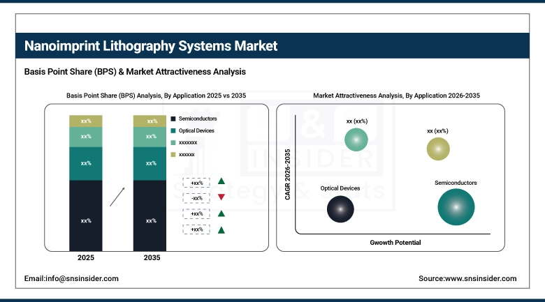
By Application: Dominant – Semiconductors (46.30% in 2025 → 50.80% in 2035); Fastest-Growing – Semiconductors (46.30% in 2025 → 50.80% in 2035)
-
By End-User: Dominant – Semiconductor Foundries (42.60% in 2025 → 48.30% in 2035); Fastest-Growing – Semiconductor Foundries (42.60% in 2025 → 48.30% in 2035)
-
By Technology: Dominant – UV-based Nanoimprint Lithography (51.80% in 2025 → 56.10% in 2035); Fastest-Growing – UV-based Nanoimprint Lithography (51.80% in 2025 → 56.10% in 2035)
By Application: Semiconductors (Dominant and Fastest-Growing Segment)
Semiconductors capture a significant portion of the application segment, owing to its widespread use for advanced chip fabrication, miniaturized device, and next-generation electronic component manufacturing processes. This segment continues to hold a dominant position with steady growth drivers due to continuous innovation in semiconductor design and ever-increasing demand for high-performance computing systems.
By Type: UV-based Nanoimprint Lithography (Dominant) and Hot Embossing (Fastest-Growing)
UV-based Nanoimprint Lithography holds the largest market share due to the UV-based technique providing high resolution (sub-10nm) patterning, high throughput, and the wide adoption of the technique in the semiconductor fabrication and advanced optical devices. With its capability of offering nanoscale accuracy over what are sustainable production scales, it is the dominant technology segment across key industrial applications. On the contrary, Hot Embossing is identified as a fast-growing segment propelled by its affordability, more efficient process, and increasing application in microfluidics and biomedical device applications as well as for prototyping currently translating in consecutive gradual acceptance in both research and industrial environments.
By End-User: Semiconductor Foundries (Dominant and Fastest-Growing End-User Segment)
The end-user segment is dominated by semiconductor foundries due to their crucial nature in large-scale chip manufacturing, operation at advanced nodes, and extensive global supply chain. Continued growth in this segment is also being driven by increased investment in fabrication capacity and a tightening focus on high-precision manufacturing processes.
By Technology: UV-based Nanoimprint Lithography (Dominant and Fastest-Growing Technology Segment)
the Nanoimprint Lithography segment is expected to lead the market owing to greater nanoscale patterning accuracy and cost efficiency coupled with a well-established adoption in high-volume semiconductor and photonics manufacturing. As, more and more used in advanced fabrication processes and next-generation electronic device fabrication, it further strengthens its leading market position and fast growth.
Nanoimprint Lithography Systems Market Regional Highlights:
-
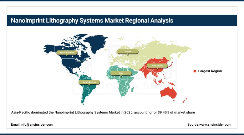
Asia-Pacific (Dominant – 39.40% in 2025 → 44.30% in 2035, CAGR 10.83%)
-
North America (28.60% in 2025 → 25.20% in 2035, CAGR 8.16%)
-
Europe (22.90% in 2025 → 20.50% in 2035, CAGR 8.34%)
-
Latin America (5.10% in 2025 → 4.10% in 2035, CAGR 7.16%)
-
Middle East & Africa (Fastest-Growing – 4.00% in 2025 → 5.90% in 2035, CAGR 13.79%)
Asia-Pacific Nanoimprint Lithography Systems Market Insights:
Asia Pacific holds the largest market share in the Nanoimprint Lithography Systems Market due to its robust semiconductor manufacturing ecosystem, increased adoption of new nanofabrication technologies, and significant research and development spending in this region. The increasing role of major foundries, electronics giants and display manufacturers makes countries like China, Japan, South Korea and Taiwan the key contributors. Conducive governmental schemes for semiconductor self-reliance and technology advancement in the region also speeds up the market growth. Moreover, the growing demand for high-performance chips, compact electronic devices, and advanced optical components is driving the use of nanoimprint lithography systems across Asia-Pacific.
Get Customized Report as per Your Business Requirement - Enquiry Now
China Nanoimprint Lithography Systems Market Insights:
China is a key driver and dominating country in the Nanoimprint Lithography Systems Industry owing to a well-established semiconductor manufacturing ecosystem in the country, continued support from the government towards advanced lithography technologies in the country coupled with rapid development in domestic chip production capabilities. China seizes on the regional markets as increasing investments in nanotechnology research and growing demand for high-precision electronics and photonic devices are strengthening its leadership position.
North America Nanoimprint Lithography Systems Market Insights:
North America is the fastest growing region in the Nanoimprint Lithography Systems Market, driven by strong investments in advanced semiconductor fabrication, increasing adoption of next-generation nanotechnology, and the presence of leading technology companies and research institutions. Rising demand for high-performance computing, AI chips, and miniaturized electronic components is further accelerating market growth in the region. Additionally, significant government funding for semiconductor innovation and growing collaboration between industry and academia are boosting the adoption of nanoimprint lithography systems across North America.
U.S. Nanoimprint Lithography Systems Market Insights:
The North America U.S. Nanoimprint Lithography Systems Market is a major hub in the semiconductor industry with one of the largest electronics manufacturing industry, the advanced R&D infrastructure they developed for new technology, the availability of skilled labor, and the presence of major technology companies. This market leadership is only reinforced by continual advances in nanofabrication and surging demand for high-performance chips.
Europe Nanoimprint Lithography Systems Market Insights:
Europe Nanoimprint Lithography Systems Market is witnessing stable growth due to steady advancements in semiconductor research, increasing adoption of nanofabrication technologies, and strong support from government-funded innovation programs. The region benefits from the presence of established research institutes, photonics companies, and precision engineering firms that are actively developing next-generation lithography solutions. Additionally, rising demand for miniaturized electronic components, optical devices, and advanced sensors is contributing to gradual market expansion. Collaborative R&D initiatives and growing focus on technological sovereignty in semiconductor manufacturing are further supporting the consistent growth of the Nanoimprint Lithography System across Europe.
Germany Nanoimprint Lithography Systems Market Insights:
Nanoimprint Lithography System Market size in Germany is led by the strong semiconductor equipment industry, high-end research infrastructure, and keeps the lead in precision engineering and technology innovation. It is a home to some of the key photonics and lithography technology companies which continuously pushes for the advancement and the implementation of state-of-the-art nanoimprint technology..
Latin America Nanoimprint Lithography Systems Market Insights:
The Latin America Nanoimprint Lithography Systems Industry is forecast to grow at a steady pace as this region has witnessed increased investments in semiconductor research, slow adaptations for advanced nanofabrication technologies and continuous development of electronics manufacturing in the region. Brazil and Mexico actively strengthen industrial and academic research on microelectronics and photonics to play more crucial roles in regional supply chains. Market growth is also aided by rising demand in consumer electronics, automotive electronics, and controlled sensing technologies. Furthermore, steady adoption in Latin America of nanoimprint lithography systems are attributed to partnerships with international semiconductor firms, and growing interest in indigenous integrated circuit technology.
Brazil Nanoimprint Lithography Systems Market Insights:
Brazil Nanoimprint Lithography Systems Industry is growing steadily due to increasing investments in semiconductor research, expanding electronics manufacturing, and rising adoption of advanced nanotechnology solutions. Government initiatives supporting industrial modernization and growing collaboration with global technology firms are further driving market development in the country.
Middle East & Africa Nanoimprint Lithography Systems Market Insights:
Middle East & Africa Nanoimprint Lithography Systems Industry Increasing Investments in Technology Infrastructure, Growing Focus on Semiconductor Research and Slow but steady Adoption on Advanced Manufacturing Processes are driving the gradual Growth of MEA Nanoimprint Lithography System market Across the region, developing the expanding interest in electronics innovation coupled with growing collaboration with global tech companies are also supporting market growth.
Israel Nanoimprint Lithography Systems Market Insights:
Israel Leads the MEA Nanoimprint Lithography Systems Industry with Robust Semiconductor R&D and Photonics Innovation, UAE and Saudi Arabia Emerging Owing to Big Technology Investments and Diversification Initiatives The Nanoimprint Lithography System Market report discusses the market share of the leading companies and penetrations level of the significant companies amongst the targeted end-use verticals in the different regions.
Nanoimprint Lithography Systems Market Competitive Landscape:
EV Group (EVG) is a global supplier of semiconductor production equipment, offering wafer bonding, lithography and nanoimprint lithography solutions. The company provides high precision process technologies for advanced chip manufacturing, MEMS, and photonics device applications. EVG is a recognized innovator that focuses on developing next-generation semiconductor fabrication and high-volume nanoimprint lithography systems.
-
In October 2025 — EV Group (EVG) received the “30 Years Nanoimprint Grand Achievement Award” at the 24th International Conference on Nanoimprint and Nanoprint Technology (NNT) in Dana Point, California, in recognition of its pioneering contributions to nanoimprint lithography, including the development and commercialization of high-volume manufacturing tools enabling global industrial adoption of NIL technology.
Nanoimprint Lithography Systems Companies are:
-
EV Group (EVG)
-
Canon Inc.
-
Nanonex Corp.
-
Obducat AB
-
NIL TECHNOLOGY (NILT)
-
AMO GmbH
-
Stensborg A/S
-
Germanlitho
-
FUJIFILM Corporation
-
SCIVAX Corporation
-
GuangDuo Nano
-
Shin-Etsu Engineering
-
Seiwa Optical Co., Ltd.
-
Litho Tech Japan
-
SVG Optronics
-
Wuwei Zhizao
-
PRINANO Technology
-
EnTeng Electronics
| Report Attributes | Details |
|---|---|
| Market Size in 2025 | USD 144.007 Million |
| Market Size by 2035 | USD 358.32 Million |
| CAGR | CAGR of 9.55% From 2026 to 2035 |
| Base Year | 2025 |
| Forecast Period | 2026-2035 |
| Historical Data | 2022-2024 |
| Report Scope & Coverage | Market Size, Segments Analysis, Competitive Landscape, Regional Analysis, DROC & SWOT Analysis, Forecast Outlook |
| Key Segments | • By Type(Hot Embossing (HE), UV-based Nanoimprint Lithography (UV-NIL), Micro Contact Printing (µ-CP)) • By Application(Semiconductors, Optical Devices, Biotechnology and Consumer Electronics) • By End-User(Semiconductor Foundries, Photonics & Optical Manufacturers, Research & Academic Institutes, Medical Device Companies and Display OEMs) • By Technology(Thermal Nanoimprint Lithography, UV-based Nanoimprint Lithography, Hybrid / Advanced NIL Systems and Roll-to-Plate / Step-and-Repeat NIL Systems) |
| Regional Analysis/Coverage | North America (US, Canada), Europe (Germany, UK, France, Italy, Spain, Russia, Poland, Rest of Europe), Asia Pacific (China, India, Japan, South Korea, Australia, ASEAN Countries, Rest of Asia Pacific), Middle East & Africa (UAE, Saudi Arabia, Qatar, South Africa, Rest of Middle East & Africa), Latin America (Brazil, Argentina, Mexico, Colombia, Rest of Latin America). |
| Company Profiles | EV Group (EVG), Canon Inc., SUSS MicroTec SE, Nanonex Corp., Obducat AB, NIL TECHNOLOGY (NILT), AMO GmbH, Stensborg A/S, Germanlitho, Morphotonics, FUJIFILM Corporation, SCIVAX Corporation, GuangDuo Nano, Shin-Etsu Engineering, Seiwa Optical Co., Ltd., Litho Tech Japan, SVG Optronics, Wuwei Zhizao, PRINANO Technology, EnTeng Electronics. |
Frequently Asked Questions
Asia-Pacific dominated the Nanoimprint Lithography Systems Market in 2025.
The “UV-based Nanoimprint Lithography (UV-NIL)” segment dominated during the projected period.
Growing demand for semiconductor miniaturization, cost-effective alternative to EUV lithography, rising adoption in memory and photonics devices, increasing R&D investments in nanofabrication, expansion of AI/5G/HPC technologies, and growing applications in biotechnology and advanced optical and display systems are the key drivers of the Nanoimprint Lithography Systems Market.
The Market was valued at USD 144.007 Million in 2025 and is projected to reach USD 358.32 Million by 2035.
The Market is expected to grow at a CAGR of 9.55% during 2026–2035.
Get in Touch
