Sputtering Equipment Market Report Scope & Overview:
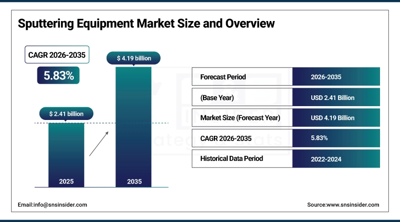
The Sputtering Equipment Market size is estimated at USD 2.41 Billion in 2025 and is projected to reach USD 4.19 Billion by 2035, growing at a CAGR of 5.83% during the forecast period 2026–2035.
The Sputtering Equipment Market analysis report offers a comprehensive analysis of market dynamics, technology developments, and application trends in the market. The demand for sputtering equipment is driven by semiconductor manufacturing, high growth rate in the electronics and display industry, increased adoption of thin-film deposition technologies, and growth in solar photovoltaic technologies.
The usage of sputtering equipment is witnessing increased adoption in semiconductor manufacturing facilities, display manufacturing units, and solar panel manufacturing facilities, with increased utilization driven by advanced semiconductor fabrication.
Market Size and Growth Projection:
-
Market Size in 2025: USD 2.41 Billion
-
Market Size by 2035: USD 4.19 Billion
-
CAGR: 5.83% from 2026 to 2035
-
Base Year: 2025
-
Forecast Period: 2026–2035
-
Historical Data: 2022–2024
To Get more information on Sputtering Equipment Market - Request Free Sample Report
Sputtering Equipment Market Trends:
-
Increasing demand in semiconductor manufacturing and advanced node fabrication is boosting the adoption rate of high-precision sputtering systems.
-
Increasing expansion in electronics, display panels including LCD and OLED, and consumer devices is creating a high demand for thin film deposition technology.
-
Increasing investments in semiconductor fabs and government initiatives in domestic chip manufacturing are creating a high demand for sputtering systems.
-
Rapidly growing solar photovoltaic industry is boosting the adoption rate of sputtering systems in thin film solar cell manufacturing.
-
Increasing advancements in magnetron, plasma-based, and ion beam sputtering technology are significantly improving deposition efficiency.
-
Increasing focus on automation and AI-enabled sputtering systems is improving production efficiency.
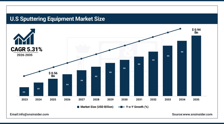
U.S. Sputtering Equipment Market Size Outlook:
The U.S. Sputtering Equipment Market is expected to grow from around USD 0.56 Billion in 2025 to USD 0.94 Billion in 2035, growing at a CAGR of 5.31%. The market is expected to grow due to increased activities in semiconductor manufacturing, expansion of advanced fabrication facilities in the country, increased investments in domestic chip manufacturing initiatives, growing demand from electronics and display manufacturing industries, and continuous improvements in thin film deposition technology used in various industrial and research applications.
Sputtering Equipment Market Growth Drivers:
-
Rising demand for semiconductors, electronics, and solar industries for advanced sputtering equipment.
The rising demand for high-end semiconductors, flat panel displays, photovoltaic cells, and other electronic devices is one of the major growth drivers of the Sputtering Equipment Industry. Semiconductor manufacturers, electronic foundries, solar industries, and other players in these industries are increasingly adopting physical vapor deposition techniques, such as magnetron sputtering technology, for precise thin film coating. The rising investments in fabrication plants, along with advancements in precision coating techniques, are further accelerating the growth of the Sputtering Equipment Market.
Over 60% of semiconductor manufacturers, electronic foundries, solar industries, and other players in these industries have been utilizing sputtering equipment in 2025 for thin film coating.
Sputtering Equipment Market Restraints:
-
High equipment costs and installation complexities are restraining the widespread adoption of sputtering equipment in emerging and small-scale manufacturing facilities.
High capital investment requirements and complex installation processes are significant restraining factors in the growth of the Sputtering Equipment Industry. Magnetron sputtering and RF sputtering systems, which are advanced sputtering equipment, require a significant initial investment. This is in addition to the costs of integrating these systems into a cleanroom, maintaining them, and operating them, which requires skilled technicians and engineers. As a result, small and medium-sized semiconductor manufacturing facilities, research institutions, and electronics manufacturing facilities face financial constraints when trying to acquire high-end sputtering systems..
Sputtering Equipment Market Opportunities:
-
Expansion of semiconductor fabrication facilities, along with rising investments in advanced nodes, display technologies, and next-generation electronics, creates a major opportunity for the Sputtering Equipment Industry.
Semiconductor fabrication facilities, electronics manufacturing, and solar panel manufacturing have been witnessing increasing adoption of thin-film deposition technologies to cater to the rising need for miniaturized, highly efficient, and performance-oriented components. The government's initiatives in promoting domestic chip manufacturing, combined with the increasing association between equipment suppliers and fabrication facilities, have helped to accelerate the adoption of advanced technologies. The constant innovation in magnetron, RF, and reactive sputtering technologies, combined with the increasing need for uniform coatings and efficient production, has helped to accelerate the growth of the Sputtering Equipment Market.
More than half of the semiconductor fabrication and advanced electronics manufacturing facilities are expected to adopt advanced technologies in sputtering equipment by 2025 to support the next-generation chip manufacturing and thin-film technologies.
Segmentation Analysis:
-
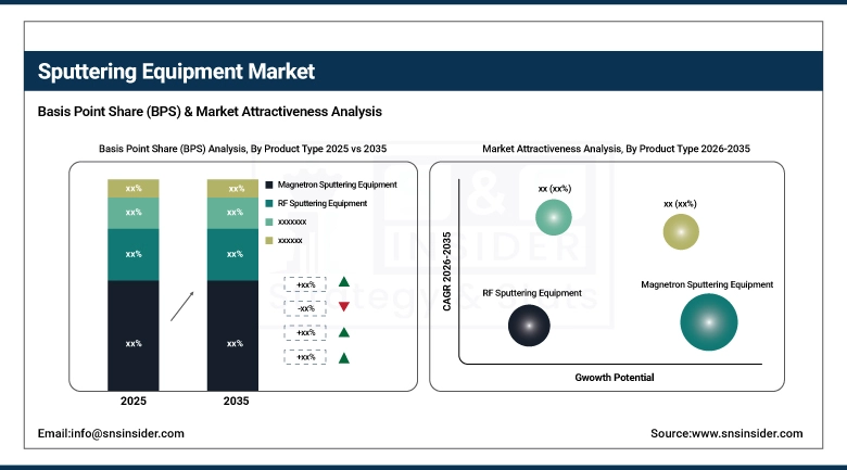
By Product Type, Magnetron Sputtering Equipment held the largest market share of 42.25% in 2025, while Reactive Sputtering Equipment is expected to grow at the fastest CAGR of 7.42% during 2026–2035.
-
By Target Material, Metal Targets dominated with a 47.21% market share in 2025, whereas Compound Targets are projected to record the fastest CAGR of 7.41% through 2026–2035.
-
By Technology, Magnetron Sputtering led with a 49.25% market share in 2025, while Plasma-Based Sputtering is expected to grow at the fastest CAGR of 8.86% during the forecast period.
-
By End-User, Semiconductor Manufacturers held the largest share of 37.12% in 2025, whereas Solar Energy Companies are anticipated to expand at the fastest CAGR of 9.05% through 2026–2035.
-
By Application, Semiconductors & Electronics dominated with a 45.25% market share in 2025, while Solar Photovoltaics is expected to grow at the fastest CAGR of 8.06% during the forecast period.
By Product Type, Magnetron Sputtering Equipment Dominate While Reactive Sputtering Equipment Grow Rapidly:
Magnetron Sputtering Equipment segment accounted for the largest market share due to its high efficiency, plasma stability, and wide acceptance in the semiconductor, electronics, and display industries. The equipment is widely used in large-scale fabrication facilities where uniform thin films, process stability, and scalability are important. The equipment's strong integration with the fabrication line and its compatibility with high-end fabrication requirements make it the preferred equipment among end-users.
Reactive Sputtering Equipment is the fastest-growing segment, with high demand from the semiconductor, optical, and energy industries for compound thin films, material engineering, and high-performance coatings. The equipment is gaining traction in research and high-end fabrication facilities, where precise control is required over the material composition and properties.
By Target Material, Metal Targets Dominate While Compound Targets Grow Rapidly:
The Metal Targets segment accounted for a dominant share of the market, primarily due to their extensive application in semiconductor processing, electronic device manufacturing, and various coating processes where they need to be highly conductive, strong, and possess consistent properties.
Compound Targets, on the other hand, is a segment that is witnessing a strong growth rate, mainly due to the increased need for compound materials, particularly in compound semiconductor devices, solar cells, displays, and optical devices. There is a growing trend toward thin films consisting of multiple compounds, along with enhanced properties such as electrical, optical, and thermal properties.
By Technology, Magnetron Sputtering Dominates While Plasma-Based Sputtering Grow Rapidly:
Magnetron Sputtering Segment: This segment accounted for the largest market share due to the efficiency and stability of the plasma generated, which can ensure the deposition of thin films over large substrates. This method has been used in many fabrication units, especially in the manufacture of semiconductors, display screens, and solar panels. This method has already been used in more than 48 operational systems in 2025.
Plasma-Based Sputtering Segment: This segment is growing rapidly due to the advancements in plasma control, which ensures higher deposition rates and greater versatility. This method has already been used in more than 22 systems in 2025, especially in advanced research centers and specialized fabrication units, which require complex coatings and materials for the development of advanced electronic and optical devices.
By End-User, Semiconductor Manufacturers Dominate While Solar Energy Companies Grow Rapidly:
The Semiconductor Manufacturers segment accounted for a large share of the market due to the wide usage of sputtering equipment in wafer fabrication and chip manufacturing, where high-precision thin-film deposition is critical in advanced semiconductor technologies.
The Solar Energy Companies segment is growing at a high rate, driven by increased investment in photovoltaic manufacturing facilities. Thin-film solar cell manufacturing using sputtering equipment is witnessing increased demand, along with a focus on clean energy technologies.
By Application, Semiconductors & Electronics Dominate While Solar Photovoltaics Grow Rapidly:
The segment of Semiconductors & Electronics accounted for a significant market share due to the wide usage of sputtering equipment in integrated circuits, microchips, and other electronic devices where smooth and high-quality thin films are required.
The segment of Solar Photovoltaics is growing at a high rate due to the increased demand for renewable energy and developments in thin-film solar cell technology. Investments in solar manufacturing infrastructure and increased efficiency in deposition are contributing to the usage of sputtering equipment in this segment.
Regional Insights
Asia-Pacific Sputtering Equipment Market Insights:
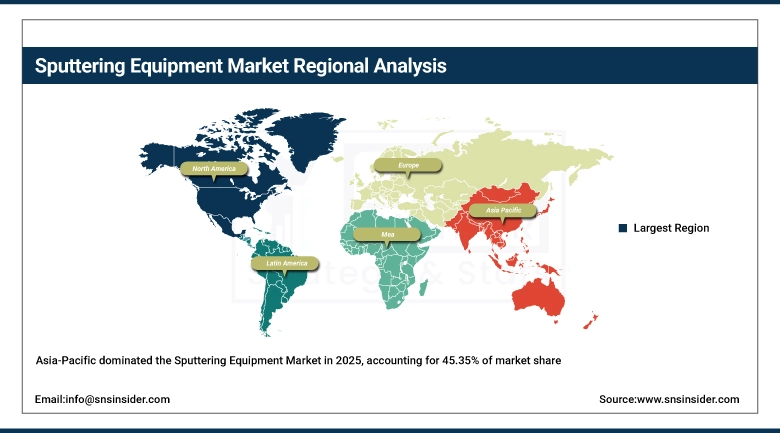
The Asia-Pacific Sputtering Equipment Market holds the largest market share, i.e., 45.35% in 2025 and the fastest-growing market, which is expected to grow at a CAGR of 6.62% during the period of 2026-2035. The market is driven by the rapid growth of semiconductor fabrication centers, increasing electronics manufacturing, and rising investment in display and solar photovoltaic segments in countries such as China, Japan, Korea, and India. The presence of foundries, increasing demand for consumer electronics, and government initiatives toward semiconductor self-sufficiency in these countries have propelled the market toward robust growth.
Get Customized Report as per Your Business Requirement - Enquiry Now
China Sputtering Equipment Market Insights:
The market in China is driven by the rapid growth of semiconductor fabrication centers, increasing electronics manufacturing, and rising investment in display and solar photovoltaic segments. The presence of robust government initiatives toward semiconductor self-sufficiency, large-scale investment in fabrication centers, and advanced manufacturing technologies have propelled the market toward robust growth.
North America Sputtering Equipment Market Insights:
North America's sputtering equipment market is substantially shaped by its thriving semiconductor fabrication sector, a highly developed electronics industry, and the concentration of major semiconductor fabrication facilities in the United States and Canada. The expansion of the sputtering equipment industry in this region is driven by the application of magnetron sputtering and RF sputtering systems in semiconductor fabs, alongside the growth of domestic semiconductor chip manufacturing. Moreover, North America's strong position in the market is bolstered by the presence of established equipment manufacturers, significant research and development capabilities, and continuous technological progress in thin-film deposition processes.
U.S. Sputtering Equipment Market Insights:
The U.S. Sputtering Equipment Industry is driven by large-scale semiconductor fabrication activities, increased domestic semiconductor chip manufacturing, and strong semiconductor equipment demand from various electronics, aerospace, and defense sectors. The expansion of advanced semiconductor manufacturing facilities, the development of next-generation semiconductor technologies, and collaboration between semiconductor equipment manufacturers and semiconductor companies are driving growth in the U.S. Market. In addition, the increasing focus on technological innovation and efficiency in semiconductor processes is strengthening the U.S.'s position in this area.
Europe Sputtering Equipment Market:
The Europe Sputtering Equipment Industry is influenced by a well-established industry base, a strong research and development scene, and growing demand from various sectors including semiconductors, automotive electronics, and renewable energy. Countries including Germany, France, and the Netherlands are at the forefront of adopting sputtering equipment technology due to their highly developed industry base and strong association between equipment manufacturers and research facilities. Growing initiatives in semiconductors, focus on high-precision engineering technology, and growing investments in renewable energy technology are contributing to steady growth in the Europe Market.
Germany Sputtering Equipment Market Insights:
Germany is one of the key markets in Europe in terms of sputtering equipment due to its strong engineering prowess, highly developed semiconductor equipment industry, and high demand from automotive electronics and industrial manufacturing sectors. Growing investments in next-generation semiconductor fabrication technology, high adoption of advanced sputtering equipment technology, and strong association between research facilities and industry players are contributing to steady growth in the Germany Sputtering Equipment Industry.
Latin America Sputtering Equipment Market Insights:
The Latin America market is witnessing steady growth with increased investments in electronics manufacturing, growth in industrialization, and gradual adoption of advanced technologies in thin films. Countries such as Brazil and Mexico are witnessing increased demand in automotive electronics, solar energy, and consumer electronics segments. Improving manufacturing infrastructure, increased participation in global supply chains, and increased awareness of advanced technologies are contributing to the growth of the sputtering equipment market in Latin America.
Middle East and Africa Sputtering Equipment Market Insights:
The Middle East & Africa sputtering equipment industry is witnessing growth with increased investments in electronics manufacturing, gradual growth in semiconductor infrastructure, and increased adoption of advanced thin film technologies. Improving infrastructure, increased growth in industrialization, and increased demand in segments such as solar energy, automotive, and consumer electronics are contributing to growth in this region. Countries such as the UAE, Saudi Arabia, and South Africa are witnessing growth in this region, driven by infrastructure development, increased demand in segments like solar energy, and increased awareness of advanced technologies in thin films.
Sputtering Equipment Market Competitive Landscape:
Applied Materials, Inc. is a leading American semiconductor equipment manufacturer based in the US, having a strong portfolio in sputtering equipment (PVD) in the areas of semiconductor manufacturing, display, and electronics device manufacturing. The company specializes in advanced deposition technology solutions that offer precise thin film control and high throughput capacity in next-generation chip production. The company has strong R&D capabilities and a global presence across top semiconductor manufacturing facilities around the world.
-
In September 2025, Applied Materials, Inc. expanded its advanced PVD portfolio with next-generation deposition platforms designed for sub-5nm nodes, improving film precision, process control, and throughput for leading semiconductor manufacturers.
Lam Research Corporation is a renowned semiconductor equipment company based in the United States, primarily focused on wafer fabrication technologies such as plasma-based deposition and etch tools that work in conjunction with sputtering tools. The company provides solutions for advanced thin film layering and precision manufacturing, with strong ties to leading foundries and integrated device manufacturers. Lam Research focuses on innovation and integration in semiconductor processes, allowing for more efficient and effective processes in leading-edge semiconductor fabs.
-
In August 2025, Lam Research Corporation introduced upgraded plasma deposition platforms with enhanced uniformity control and improved process stability to support advanced node semiconductor fabrication.
ULVAC, Inc. is a Japan-based company that is a supplier of vacuum and thin-film deposition systems. The company is a leader in sputtering technologies for the semiconductor industry, electronics, flat panels, and energy fields. The company provides a wide array of magnetron sputtering systems, RF sputtering systems, and reactive sputtering systems for high-precision thin-film processing and industrial-scale production. The company is skilled in the field of vacuum engineering and provides diverse application solutions for different industries.
-
In July 2025, ULVAC, Inc. launched enhanced magnetron sputtering systems with improved deposition efficiency and vacuum stability, targeting semiconductor, display, and advanced coating applications.
Sputtering Equipment Companies are:
-
Applied Materials, Inc.
-
Lam Research Corporation
-
Tokyo Electron Limited
-
Oxford Instruments plc
-
Veeco Instruments Inc.
-
Denton Vacuum LLC
-
Kurt J. Lesker Company
-
Buhler Group
-
Singulus Technologies AG
-
CVD Equipment Corporation
-
SPTS Technologies Ltd. (KLA Corporation)
-
Advanced Energy Industries, Inc.
-
Plasma-Therm LLC
-
Canon Anelva Corporation
-
Hitachi High-Tech Corporation
-
Showa Shinku Co., Ltd.
-
ULVAC Cryogenics Inc.
-
Trion Technology Inc.
| Report Attributes | Details |
|---|---|
| Market Size in 2025 | USD 2.41 Billion |
| Market Size by 2035 | USD 4.19 Billion |
| CAGR | CAGR of 5.83% From 2026 to 2035 |
| Base Year | 2025 |
| Forecast Period | 2026-2035 |
| Historical Data | 2022-2024 |
| Report Scope & Coverage | Market Size, Segments Analysis, Competitive Landscape, Regional Analysis, DROC & SWOT Analysis, Forecast Outlook |
| Key Segments | • By Product Type (RF Sputtering Equipment, DC Sputtering Equipment, Magnetron Sputtering Equipment, Reactive Sputtering Equipment, Others) • By Target Material (Metal Targets, Compound Targets, Ceramic Targets, Alloy Targets, Others) • By Technology (Physical Vapor Deposition (PVD), Magnetron Sputtering, Ion Beam Sputtering, Plasma-Based Sputtering, Others) • By End-User (Semiconductor Manufacturers, Electronics & Semiconductor Foundries, Solar Energy Companies, Research & Academic Institutes, Others) • By Application (Semiconductors & Electronics, Solar Photovoltaics, Displays, Optical Coatings, Others) |
| Regional Analysis/Coverage | North America (US, Canada), Europe (Germany, UK, France, Italy, Spain, Russia, Poland, Rest of Europe), Asia Pacific (China, India, Japan, South Korea, Australia, ASEAN Countries, Rest of Asia Pacific), Middle East & Africa (UAE, Saudi Arabia, Qatar, South Africa, Rest of Middle East & Africa), Latin America (Brazil, Argentina, Mexico, Colombia, Rest of Latin America). |
| Company Profiles | Applied Materials, Inc., Lam Research Corporation, ULVAC, Inc., Hitachi High-Tech Corporation, Canon Anelva Corporation, Tokyo Electron Limited, Oxford Instruments plc, Veeco Instruments Inc., Denton Vacuum LLC, Kurt J. Lesker Company, AJA International, Inc., Buhler Group, Singulus Technologies AG, Oxford Instruments Plasma Technology, Angstrom Engineering Inc., CVD Equipment Corporation, SPTS Technologies Ltd. (KLA Corporation), Advanced Energy Industries, Inc., Plasma-Therm LLC. |
Frequently Asked Questions
Asia Pacific dominated the market in 2025 with 45.35% share, while Asia-Pacific is also the fastest-growing region with cagr of 6.32%, driven by rapid expansion of semiconductor manufacturing, electronics production, and solar energy investments.
Magnetron Sputtering Equipment dominated with a 42.25% share in 2025, while Reactive Sputtering Equipment is projected to grow at the fastest CAGR of 7.42% during 2026–2035.
Growth is driven by rising semiconductor manufacturing, increasing demand from electronics and display industries, expansion of solar photovoltaics, and advancements in thin-film deposition technologies.
The market is valued at USD 2.41 Billion in 2025 and is projected to reach USD 4.19 Billion by 2035.
The Sputtering Equipment Market is projected to grow at a CAGR of 5.83% during 2026–2035.
Get in Touch
