Photomask Market Report Scope & Overview:
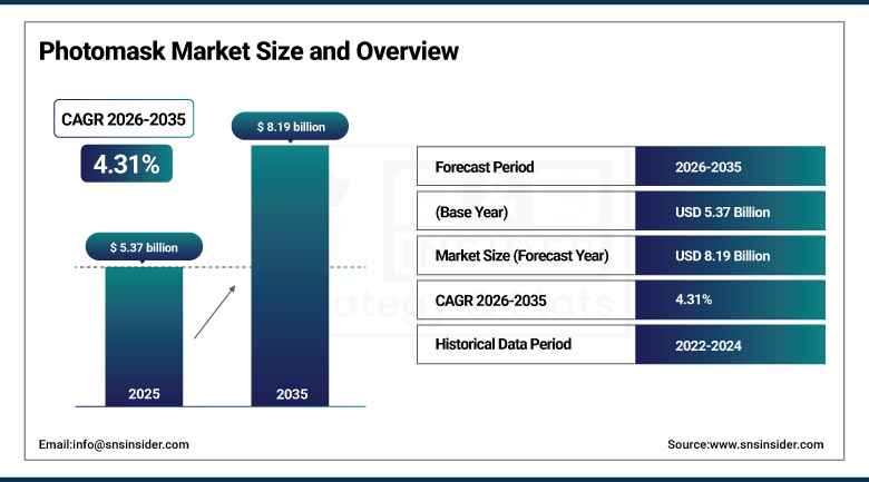
The Photomask Market was valued at USD 5.37 billion in 2025 and is expected to reach USD 8.19 billion by 2035, growing at a CAGR of 4.31% from 2026-2035.
The growth of the photomask market is fueled by an increase in the need for advanced semiconductor chips in consumer electronics, automobiles, telecommunication, and industrial applications. The need for advanced integrated circuit technology owing to the increasing use of artificial intelligence, 5G, and IoT is another factor that is contributing to the growth of the industry. Moreover, the continued expansion of the semiconductor foundry capacity along with continuous investment in advanced lithography solutions is boosting the market growth further. Demand for high-performance computing as well as electric cars is adding to this trend.
According to the International Energy Agency, global electric car sales exceeded 14 million units in 2023, significantly increasing semiconductor content per vehicle, which in turn drives higher demand for photomasks used in automotive chip fabrication.
Market Size and Forecast
-
Market Size 2026E: USD 5.60 Billion
-
Market Size 2035: USD 8.19 Billion
-
CAGR (2026-2035): 4.31%
-
Fastest Growing Market: North America
-
Largest Market: Asia Pacific
To Get more information on Photomask Market - Request Free Sample Report
Photomask Market Trends
-
Rising demand for advanced semiconductor manufacturing and miniaturized electronic components is driving the photomask market.
-
Growing adoption across consumer electronics, automotive electronics, and high-performance computing applications is boosting market growth.
-
Expansion of AI, 5G, IoT, and data center technologies is fueling demand for advanced chip fabrication.
-
Increasing focus on high-resolution lithography and precision pattern transfer is shaping adoption trends.
-
Advancements in EUV lithography, mask inspection systems, and defect-free photomask technologies are enhancing semiconductor production efficiency.
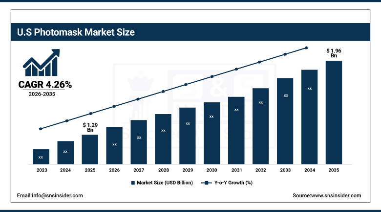
U.S. Photomask Market Size Outlook
The U.S. Photomask Market was valued at USD 1.29 billion in 2025 and is expected to reach USD 1.96 billion by 2035, growing at a CAGR of 4.26% from 2026-2035.
The United States photomask market has witnessed robust growth owing to the increase in demand from semiconductor manufacturers along with the constant investment in new manufacturing techniques of semiconductors. The applications of artificial intelligence, data center, automotive electronics, and telecommunication have increased the complexity and manufacture of chips. The robust government support for semiconductor production in the country and technological innovations have supported market growth.
The Intel Corporation announced multi-billion-dollar investments in new fabs in the U.S. and Europe, aimed at increasing advanced chip manufacturing capacity for AI and high-performance computing applications, directly boosting demand for advanced photomask technologies.
Photomask Market Segment Analysis
-
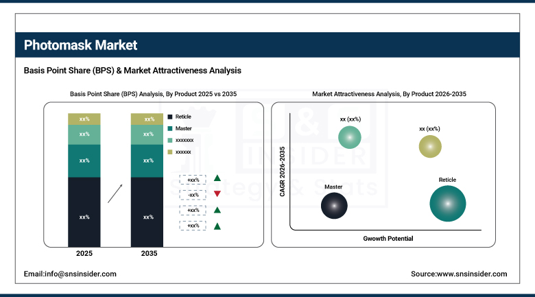
By Product, Reticle segment dominated the photomask market in 2025 with 57.34% share; Master segment is the fastest growing.
-
By Application, Displays segment dominated the photomask market in 2025 with 31.68% share; MEMS segment is the fastest growing.
-
By Technology, Optical Lithography segment dominated the photomask market in 2025 with 64.25% share; EUV Lithography segment is the fastest growing.
-
By End Use, Consumer Electronics segment dominated the photomask market in 2025 with 42.17% share; Automotive segment is the fastest growing.
By Product, reticle segment dominates the photomask market, master segment is the fastest growing
The reticle segment leads the photomask market owing to its indispensable use in semiconductor manufacturing processes and high-end lithography techniques. The reticles find widespread application in lithography processes to transfer very accurate circuit patterns on wafers in integrated circuit fabrication processes. Rising demands for smaller electronic parts and semiconductor chips also provide strong impetus. High accuracy, suitability in large scale production and application in consumer electronics devices and communication equipment have played a key part in making reticle segment dominate the global photomask industry in 2025.
Master segment is the fastest growing in the photomask market due to rising demand for high accuracy masters used in high-end semiconductor fabrication processes and manufacturing of displays. Advancements in integrated circuits design and rising use of advanced generation manufacturing technology in the process have fueled growing demand for master photomasks. The photomasks enable higher accuracy during pattern replication and transfer in lithography operations. Investments in semiconductor fabrication processes and advances in micro-fabrication technologies have been fueling the growing demand for masters globally.
By Application, displays segment dominates the photomask market, MEMS segment is the fastest growing
Displays segment dominates the photomask market owing to the escalating number of televisions, smartphones, tablets, laptops, and superior display panels across the globe. Photomasks play a critical role in the production process that involves patterning the circuits within liquid crystal displays, OLEDs, and micro-LED displays. Furthermore, escalating consumer demand for high-resolution and power-saving display solutions contributes immensely to the dominance of the market. Expansion within the consumer electronics industry and innovation in display manufacturing technology are two other reasons behind the dominance of the displays segment within the photomask market in 2025.
MEMS segment is the fastest growing in the photomask market due to the rising demand for microelectromechanical systems in applications such as automotive, healthcare, consumer electronics, and industrial sectors. Microelectromechanical systems are made using highly sophisticated photolithography techniques, and hence, there is an ever-growing demand for photomasks that facilitate the same. Growing demand for wearable and other IoT devices is another key factor driving the fast-paced growth of the MEMS application segment.
By Technology, optical lithography dominates the photomask market, EUV lithography is the fastest growing
Optical lithography dominates the photomask market because of its extensive application in semiconductor and display fabrication processes, where pattern transfer technique is essential and must be affordable and reliable. Its usage allows mass production of chips while providing compatibility with existing facilities. In addition, growing integration of circuit boards in consumer electronics, communication systems, and industries will support the growth prospects. Constant development that provides better resolution, efficiency, and productivity plays a significant role in the global dominance of optical lithography technology in 2025.
EUV lithography is the fastest growing segment in the photomask market due to the increasing demand for advanced semiconductor technology and miniaturization of chips. This technology ensures high precision for future ICs with higher performance and reduced energy consumption. Growing investments in artificial intelligence, high-performance computing, and 5G networks have boosted adoption. Moreover, growing capacities of semiconductors fabrication and an emphasis on creating compact ICs ensure steady global growth of EUV lithography.
By End Use, consumer electronics segment dominates the photomask market, automotive segment is the fastest growing
Consumer Electronics dominates the photomask market owing to the high global demand for smartphones, tablets, laptops, televisions, gaming consoles, and wearables. These photomasks find their application in the manufacture of the semiconductor chips and the display panels used in the aforementioned applications. Additionally, rapid technology developments coupled with continuous product upgrades are adding to the growth in production within the electronics industry. The preference towards miniaturized, performance-enhanced, and power-saving electronics is also aiding the dominance of the segment.
Automotive segment is the fastest growing in the photomask market owing to the incorporation of semiconductors, sensors, and sophisticated electronics within automobiles. Increased use of electric vehicles, autonomy systems, and driver assistance systems has resulted in rising demand for semiconductors. Photomasks have a vital role to play in producing automotive semiconductors and MEMS sensors. Increased investments by automobile manufacturers in electric vehicles and safety/communication features have also been boosting the growth of this market.
Regional Analysis
|
Region |
Major Country |
Share within Region (%) |
|---|---|---|
|
North America |
United States |
91.8% |
|
Europe |
United Kingdom |
22.4% |
|
Asia Pacific |
China |
46.7% |
|
Middle East & Africa |
UAE |
11.8% |
|
Latin America |
Brazil |
47.9% |
North America Photomask Market Insights
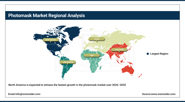
North America is expected to witness the fastest growth in the photomask market over 2026–2035, with a projected CAGR of 5.94%, owing to growing investments in local semiconductor manufacturing and fabrication facilities. Demand for high-performance semiconductors in sectors such as artificial intelligence, data centers, automotive electronics, and telecom is driving the growth of the photomask market. Various government schemes promoting semiconductor production and robust supply chains are propelling the photomask market ahead. Availability of leading tech firms and ongoing R&D efforts in lithographic processes also play an important role in driving regional market growth.
Get Customized Report as per Your Business Requirement - Enquiry Now
Europe Photomask Market Insights
Europe holds a notable position in the photomask market because of the rising demands for semiconductors within the automotive, industrial automation, healthcare, and telecom industries. The presence of automotive semiconductor manufacturers as well as increased usage of advanced driver assistance systems is fueling efforts towards semiconductor manufacturing activities. Increased investments in R&D activities and increased emphasis on innovation is adding to the growth potential of this market. Growing investments in electric vehicles and intelligent industrial applications have resulted in rising demand for high-performing integrated circuits; hence, photomask technology usage is increasing.
Asia Pacific Photomask Market Insights
In 2025, Asia Pacific dominated the photomask market and accounted for 44% of revenue share owing to the presence of prominent semiconductor fabrication centers in countries like China, Taiwan, South Korea, and Japan. The rapid development in consumer electronics manufacturing and rising demand for innovative semiconductor components are driving growth in the regional market. Investments made towards semiconductor fabrication units and state-of-the-art lithography techniques have enabled further regional dominance. Rising demand for 5G, AI, and EV has also driven the demand for advanced integrated circuitry, thereby boosting the growth of photomask manufacturing in the region.
Middle East & Africa and Latin America Photomask Market Insights
Middle East & Africa and Latin America regions are witnessing gradual growth in the photomask market owing to digitalization trends and increasing needs for consumer electronics and communications equipment. Growing industrialization and investment into telecommunication network facilities have increased semiconductor consumption within both these regions. Countries within these regions are looking into the modernization of technology and electronics production capabilities, resulting in increased consumption of semiconductors. The increasing use of electronic systems such as smart devices, automotive electronics, and industrial automation systems will continue to boost the photomask market.
Market Dynamics
Growth Drivers: Rising semiconductor demand and consumer electronics adoption driving photomask production and technology expansion globally
An increasing demand for semiconductors in consumer electronics, automotive technology, telecommunication devices, and industrial applications is leading to an increase in demand for photomasks. The increased production of smartphones, tablets, wearables, and high-end computers is also increasing the activity of semiconductor manufacturing. Photomasks are crucial in the lithography process used in IC manufacturing, and hence there is an increase in demand for advanced and precise photomasks. The rapid implementation of AI, 5G, and IoT technology is another major factor that is leading to increased semiconductor complexity and manufacturing activities. There are also significant investments in manufacturing semiconductor fabrication plants and lithography technologies, further driving the market growth.
Restraints: High manufacturing costs and fabrication complexity limiting adoption among smaller semiconductor manufacturers worldwide
High costs related to the manufacturing of photomasks due to their advanced nature have become a barrier for many semiconductor firms, especially small and medium-sized businesses. The cost of manufacturing such photomasks with high precision necessitates the use of highly advanced machines, materials, and processing methods. This has increased production costs. As the designs of semiconductors become more complicated, the cost involved in producing these photomasks will continue to increase since the time required to produce them becomes higher. With the continuous upgrading of photomask technology, there is an ever-increasing cost involved in its production process. Increased complexities in the manufacturing process of semiconductor technology lead to production errors and delays.
Opportunities: Expanding electric vehicle production and automotive electronics creating opportunities for advanced photomask technologies globally
The fast-growing production of electric cars and increasing penetration of cutting-edge technology in automobiles have created tremendous growth prospects for photomask producers around the world. Contemporary automobiles are incorporating semiconductors for features like driver assistances, infotainment systems, battery management systems, and even autonomous capabilities. The rising demands for semiconductors in the automotive industry are contributing to increased demand for photomask products that play an important part in chip manufacturing processes. Automobile makers are moving towards more complex electronics platforms that necessitate accurate and reliable semiconductors. Investments in the electric and smart vehicle segments will also help the market grow. Photomask companies concentrating on higher resolution photomask products can benefit from increased semiconductor needs in the automotive industry.
Recent Developments:
-
2025: DNP achieved high-NA EUV photomask resolution for beyond-2nm nodes, initiating sample supply for next-generation semiconductor development and advancing mask technology for AI and HPC chips.
-
2024: DNP began development of 2nm-generation EUV photomask manufacturing, partnering with Japan’s Rapidus project. The initiative aims to commercialize advanced lithography masks for next-generation logic chips by FY2026–2027.
-
2024: Toppan Photomask signed a joint R&D agreement with IBM to develop EUV photomasks for 2nm and High-NA lithography, supporting next-generation semiconductor nodes at Albany NanoTech and Japan facilities.
-
2023: DNP announced development of a 3nm EUV photomask manufacturing process, strengthening its advanced semiconductor lithography capabilities. The process supports next-gen chip scaling and improves pattern accuracy for high-performance logic semiconductors.
-
2023: Applied Materials expanded advanced patterning and inspection tool capabilities supporting EUV photomask ecosystem development, enabling higher precision defect detection and process control for next-generation semiconductor manufacturing.
Photomask Market Key Players are:
-
Advance Reproductions Corp.
-
Applied Materials Inc.
-
HOYA Corporation
-
Infinite Graphics Incorporated
-
KLA Corporation
-
LG Innotek Co. Ltd.
-
Nippon Filcon Co. Ltd.
-
Photronics Inc.
-
SK-Electronics Co. Ltd.
-
Toppan Photomasks, Inc.
-
Dai Nippon Printing Co., Ltd. (DNP)
-
Taiwan Mask Corporation (TMC)
-
Compugraphics International Ltd.
-
SUSS MicroTec SE
-
Veeco Instruments Inc.
-
Carl Zeiss SMT GmbH
-
Naura Technology Group Co., Ltd.
-
Newway Photomask
-
Tianjin Zhonghuan Semiconductor Co., Ltd.
-
Lasertec Corporation
Photomask Market Report Scope:
| Report Attributes | Details |
|---|---|
| Market Size in 2025 | USD 5.37 Billion |
| Market Size by 2035 | USD 8.19 Billion |
| CAGR | CAGR of 4.31% From 2026 to 2035 |
| Base Year | 2025 |
| Forecast Period | 2026-2035 |
| Historical Data | 2022-2024 |
| Report Scope & Coverage | Market Size, Segments Analysis, Competitive Landscape, Regional Analysis, DROC & SWOT Analysis, Forecast Outlook |
| Key Segments | • By Product(Reticle, Master and Other Products) • By Application(Displays, Discrete Components, Optical Devices, MEMS and Other Applications • By Technology(Optical Lithography, EUV Lithography and X-ray Lithography) • By End Use(Consumer Electronics, Automotive, Telecommunications and Healthcare |
| Regional Analysis/Coverage | North America (US, Canada), Europe (Germany, UK, France, Italy, Spain, Russia, Poland, Rest of Europe), Asia Pacific (China, India, Japan, South Korea, Australia, ASEAN Countries, Rest of Asia Pacific), Middle East & Africa (UAE, Saudi Arabia, Qatar, South Africa, Rest of Middle East & Africa), Latin America (Brazil, Argentina, Mexico, Colombia, Rest of Latin America). |
| Company Profiles | Advance Reproductions Corp., Applied Materials Inc., HOYA Corporation, Infinite Graphics Incorporated, KLA Corporation, LG Innotek Co. Ltd., Nippon Filcon Co. Ltd., Photronics Inc., SK-Electronics Co. Ltd., Toppan Photomasks, Inc., Dai Nippon Printing Co., Ltd. (DNP), Taiwan Mask Corporation (TMC), Compugraphics International Ltd., SUSS MicroTec SE, Veeco Instruments Inc., Carl Zeiss SMT GmbH, Naura Technology Group Co., Ltd., Newway Photomask, Tianjin Zhonghuan Semiconductor Co., Ltd., Lasertec Corporation. |
Frequently Asked Questions
Asia Pacific dominated the Photomask Market in 2025.
The Reticle segment dominated the Photomask Market in 2025.
The Photomask Market is expected to grow at a CAGR of 4.31% from 2026 to 2035.
Get in Touch
