Semiconductor Inspection Microscope Market Report Scope & Overview:
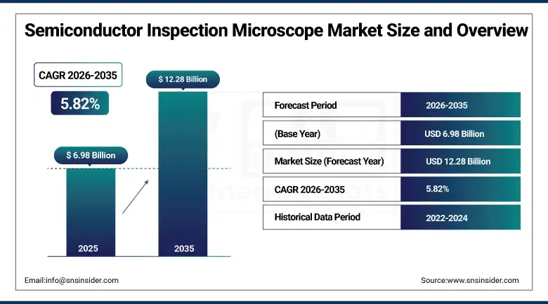
The Semiconductor Inspection Microscope Market was valued at USD 6.98 Billion in 2025 and is expected to reach USD 12.28 Billion by 2035, growing at a CAGR of 5.82% from 2026–2035.
Semiconductor inspection microscopes are witnessing growth on the international front because of the fact that manufacturers of chips are required to keep creating smaller and better chips, which in turn ensures a continuous increase in the demand for precise inspection instruments that can detect nanoscopic defects in current day semiconductor manufacturing. Nanoscale inspection of semiconductors poses challenges because regular optical microscopes have inherent issues with diffraction and thus need SEM and TEM instruments with high resolution for defect detection within the range of less than 200 nanometers and 50 picometers, respectively.
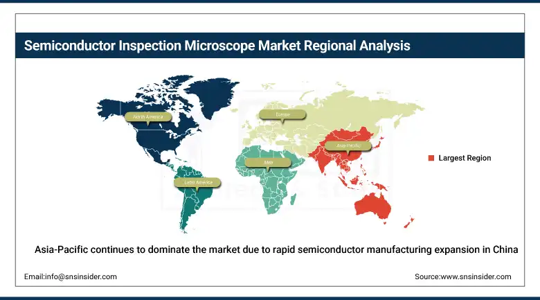
Reshoring of semiconductor production, supported by the CHIPS and Science Act, is driving demand for advanced inspection microscopes in the United States. Asia Pacific continues to dominate the market.
In September 2025, KLA Corporation launched new AI-centric semiconductor process-control solutions enabling nanoscale defect detection for advanced GPU, HBM, and heterogeneous chip architectures to support next-generation AI manufacturing.
Market Size and Forecast
-
Market Size in 2026E: USD 7.39 Billion
-
Market Size by 2035: USD 12.28 Billion
-
CAGR: 5.82% from 2026 to 2035
-
Fastest Growing Region: Asia Pacific
-
Largest Region: Asia Pacific
To Get more information On Semiconductor Inspection Microscope Market - Request Free Sample Report
Semiconductor Inspection Microscope Market Trends
-
AI and machine learning integration is enabling quicker defect identification and improved inspection efficiency across fabrication facilities.
-
Expansion microscopy is surpassing the light diffraction limit, allowing visualisation of sub-200 nanometre semiconductor structures.
-
Time-resolved electron microscopy is achieving magnifications enabling resolutions below 50 picometres in transmission electron microscopy.
-
Advanced packaging and chiplet architecture innovations are requiring increasingly precise heterogeneous integration inspection capabilities.
-
Water management infrastructure investment is supporting sustainable chip production expansion alongside inspection equipment demand.
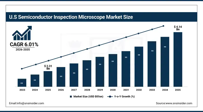
The U.S. Semiconductor Inspection Microscope Market Outlook
The U.S. Semiconductor Inspection Microscope Market was valued at USD 2.31 billion in 2025 and is expected to reach approximately USD 4.14 billion by 2035, expanding at a CAGR of 6.01% during 2026–2035.
The United States leads North American semiconductor inspection microscope revenues through the CHIPS and Science Act’s reshoring of semiconductor production and the presence of major chip manufacturers and advanced research institutions boosting demand for ultra-high-resolution inspection systems. KLA Corporation, Applied Materials, and Thermo Fisher Scientific sustain U.S. market leadership through their comprehensive inspection microscope portfolios serving advanced packaging and chiplet architecture applications across logic, memory, and heterogeneous integration use cases.
Onto Innovation showcased advanced metrology and inspection solutions at SEMICON West 2025, driving leadership in AI and next-generation semiconductor packaging inspection capability. The company, established in 2019 through the merger of Nanometric and Rudolph Technologies, delivers advanced technologies for logic, memory, advanced packaging, and specialty devices, helping manufacturers improve yield, reliability, and production efficiency across the increasingly complex semiconductor packaging landscape.
Semiconductor Inspection Microscope Market Segment Analysis
-
By Type, Electron Microscope held a 35% market share in 2025, while Scanning Probe Microscope serves specialised atomic-scale characterisation needs.
-
By Components, Hardware dominated the semiconductor inspection microscope market with 45% share in 2025, illumination, and stage systems, while Software is growing through AI-driven defect analysis integration.
-
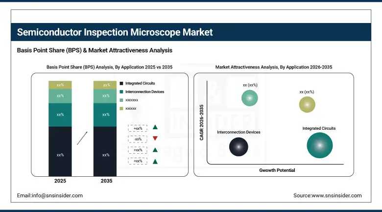
By Application, Integrated Circuits lead the market due to growing complexity making defect detection more challenging, while Memory Blocks is the fastest-growing application fuelled by rising demand for memory chips.
By Application, integrated circuits dominate, memory blocks grow fastest
The integrated circuit segment is expected to dominate the semiconductor inspection microscope market because of increasing complexities associated with it, making defect detection difficult. Semiconductor inspection microscopes play an important role in inspecting defects such as scratches, cracks, and particles in integrated circuits. They help ensure that these circuits function effectively in various electronic applications, including consumer products, automobiles, and industries, where the density of circuits is high.
Memory blocks are the fastest-growing application, fuelled by rising demand for memory chips, including high-bandwidth memory used in AI accelerator and GPU architectures whose stacked die configurations create unique inspection challenges. Each new memory chip generation that increases storage density through more aggressive cell scaling or 3D stacking creates inspection microscope procurement whose technical requirements for detecting microscopic defects within layered memory architectures exceed conventional planar semiconductor inspection demands.
By Type, electron microscopes dominate through superior resolution capability
The market share of the Electron Microscope in the semiconductor inspection microscope market was 35% in the year 2025. The electron microscope is widely used in semiconductor inspection; more particularly, the Scanning Electron Microscope is used because of its superior resolution, which can provide an inspection of both internal and external parts of a semiconductor element with a high accuracy of just a few nanometres, which is ideal for discovering small imperfections or defects in the device. The SU5000 SEM by Hitachi is known for its high-quality images along with multiple inspection and analysis modes, making it an optimal choice for semiconductor inspection purposes, whereas the Transmission Electron Microscope can be used to study the structure of crystals on the atomic level, having a resolution below 1 nanometre.
The Helios 5 UX Dual Beam by Thermo Fisher, a blend of SEM and Focused Ion Beam technologies, provides precise imaging and thorough material analysis with automated features and user-friendly interfaces improving efficiency in high-volume settings. Each new semiconductor node transition that reduces feature sizes toward 2-nanometre and beyond creates electron microscope procurement whose resolution requirements conventional optical microscopy cannot satisfy, sustaining the segment’s dominant market position as chip complexity advances.
By Components, hardware dominates through optical and illumination system complexity
Based on Component, Hardware dominated the semiconductor inspection microscope market with 45% of share in 2025. The microscope hardware, such as the optical system, illumination system, and stage, controls the market because of its high cost and complexity, with creating and producing the hardware requiring significant skill and knowledge. The optical system, the core component of a microscope, magnifies small semiconductor structures to enable accurate inspection, with Nikon’s line of Eclipse microscopes utilising sophisticated optics to offer high-quality imaging essential for semiconductor inspection.
The lighting system supplies the required illumination to improve visibility of semiconductor structures, with Carl Zeiss’s Axio Imager series including advanced lighting systems that enable a variety of inspection techniques, providing versatility for different semiconductor inspection jobs. Software is growing through AI-driven defect analysis integration, as machine learning algorithms increasingly automate defect classification and inspection workflow optimisation that complements rather than replaces the underlying hardware platform’s optical and illumination capability.
Regional Analysis
|
Region |
Major Country |
Share within Region, 2025 (%) |
|---|---|---|
|
North America |
United States |
82.5% |
|
Europe |
Germany |
22.4% |
|
Asia Pacific |
China |
44.8% |
|
Middle East & Africa |
UAE |
22.8% |
|
Latin America |
Brazil |
43.8% |
North America Semiconductor Inspection Microscope Market Insights
North America is witnessing growing adoption of semiconductor inspection microscopes driven by increasing use of AI and machine learning to detect defects with greater precision. The presence of major chip manufacturers and advanced research institutions is boosting demand for ultra-high-resolution inspection systems, with innovations in advanced packaging and chiplet architectures further requiring precise inspection capabilities. The United States accounts for approximately 82.5% of North American revenues through KLA Corporation, Applied Materials, and Thermo Fisher Scientific’s comprehensive inspection equipment manufacturing leadership.
The CHIPS and Science Act is accelerating local semiconductor production and increasing investments in inspection technologies, while rising cybersecurity concerns around chip authentication are enhancing focus on secure inspection tools. Canada’s growing semiconductor research collaboration contributes supplementary North American regional demand.
Europe Semiconductor Inspection Microscope Market Insights
Europe’s semiconductor inspection microscope market is expanding due to strict EU quality standards and increasing adoption of precision engineering solutions. The EU Chips Act is driving localised chip production and stimulating demand for advanced inspection tools, with rising demand for automotive semiconductors leading manufacturers to focus on high-reliability defect detection. Germany accounts for approximately 22.4% of European revenues through Carl Zeiss’s domestic optical and inspection equipment manufacturing leadership.
Research partnerships between universities, technology labs, and industrial manufacturers are accelerating microscopy innovation for nano-fabrication and metrology, solidifying Europe’s position as a technology-focused semiconductor inspection hub. France and the Netherlands’ advanced semiconductor equipment manufacturing capability contribute substantial secondary regional revenue.
Asia Pacific Semiconductor Inspection Microscope Market Insights
Asia-Pacific continues to dominate the market due to rapid semiconductor manufacturing expansion in China, Taiwan, South Korea, and Japan. Growing investments in EUV lithography and advanced nodes are pushing demand for extremely accurate inspection microscopes, while increasing production of EVs, IoT devices, smartphones, and consumer electronics is driving the need for superior defect detection tools. China accounts for approximately 44.8% of Asia Pacific revenues through its massive domestic semiconductor manufacturing base and government-supported fab expansion programmes.
Government subsidies and semiconductor stimulus programmes are accelerating fabs and inspection infrastructure growth across the region, while automation and AI-driven defect analytics are improving yield, speed, and inspection efficiency. Taiwan’s advanced node leadership, South Korea’s memory chip manufacturing scale, and Japan’s precision equipment manufacturing collectively sustain Asia Pacific’s dominant and fastest-growing regional trajectory.
Get Customized Report as per Your Business Requirement - Enquiry Now
MEA & Latin America Semiconductor Inspection Microscope Market Insights
The Middle East and Africa region is developing as a potential market as countries such as UAE, Saudi Arabia, and South Africa invest in semiconductor research, nanotechnology centres, and advanced electronics production. Growing initiatives in AI, robotics, smart city development, and 5G deployment are pushing demand for semiconductor inspection microscopes, with partnerships with international semiconductor firms building local knowledge and laboratory capabilities.
Latin America is experiencing gradual growth as electronics assembly, consumer device manufacturing, and automotive chip testing expand in countries like Brazil and Mexico. Industrial automation and smart manufacturing trends are increasing the need for precision quality control tools, while incentives to boost local electronics production and increasing PCB packaging and testing activities further contribute to demand for high-accuracy inspection systems.
Market Dynamics
Growth Drivers: Semiconductor reshoring and CHIPS Act domestic equipment manufacturing creating structural inspection microscope demand growth
The market for semiconductor inspection microscopes is booming owing to the necessity of chip manufacturers to develop smaller and better components consistently. Semiconductor sector recorded an important event when a total of $6.6 billion worth financial grants were awarded to TSMC in relation to the implementation of CHIPS and Science Act, where this investment, in addition to the grants for Intel and Samsung, indicates a trend of returning the manufacture of chips to the US in response to geopolitics and solid supply chain requirements.
The CHIPS and Science Act’s emphasis on domestic semiconductor equipment manufacturing, including the USD 500 million CHIPS Program Office funding opportunity announcement, will have a major effect on the Semiconductor Inspection Microscope industry by establishing a self-sustaining domestic supply chain. With increased output from domestic chip manufacturing plants, there will be higher demand for inspection microscopes sourced locally, with the close relationship between chipmakers and equipment manufacturers promoting quicker lead times and swifter troubleshooting.
Restraints: Nanoscale structure examination complexity and throughput-resolution trade-offs constraining inspection efficiency
Optical microscopes have limitations due to light diffraction that makes it hard to identify objects with sizes under 200 nanometers. The sophistication of today’s chips with complex 3D architecture poses an extra challenge in the identification of defects as there is a need to strike a balance between resolution and throughput for efficient manufacturing. Although examining a chip may take seconds, SEM analysis takes longer periods, and this could affect the efficiency of manufacturing processes.
This throughput-resolution trade-off creates manufacturing line capacity constraints where fabrication facilities must balance comprehensive defect detection against production line throughput requirements, particularly as wafer volumes increase with growing semiconductor demand across consumer electronics, automotive, and data centre AI accelerator markets. Each fabrication facility whose inspection capacity cannot keep pace with wafer production volume creates a structural bottleneck that inspection equipment manufacturers must address through faster, more automated inspection system development.
Opportunities: National innovation hubs and advanced microscopy technology development creating expanded market growth categories
Proposals to build a National Semiconductor Technology Center as well as a National Advanced Packaging Manufacturing Program intend to speed up innovations, improve supply chain robustness, and maintain the leading role of America in the semiconductor technology sphere by bringing together various stakeholders within the electronics supply chain such as equipment manufacturers, fabs, research institutions, and government organizations. Should this ambitious plan materialize, it would lead to rapid development of a semiconductor industry that would be scalable, sustainable, and locally-oriented, offering many new business opportunities in inspection equipment purchases.
Innovations in microscopy, including expansion microscopy surpassing the light diffraction limit and time-resolved electron microscopy achieving magnifications up to 2 million iterations in SEM and 50 million iterations in TEM yielding resolutions of approximately 0.5 nanometres in SEM and less than 50 picometres in TEM, are transforming semiconductor inspection. These technological developments allow for greater understanding of material characteristics and defect examination, creating premium inspection equipment categories beyond conventional resolution capability.
Recent Developments:
-
2025: KLA Corporation launched new AI-centric semiconductor process-control solutions enabling nanoscale defect detection for advanced GPU, HBM, and heterogeneous chip architectures to support next-generation AI manufacturing.
-
2025: Onto Innovation showcased advanced metrology and inspection solutions at SEMICON West 2025, driving leadership in AI and next-generation semiconductor packaging inspection capability for logic and memory applications.
-
2024: Thermo Fisher Scientific continued development of its Helios 5 UX Dual Beam system combining SEM and Focused Ion Beam technologies, providing precise imaging and thorough material analysis for advanced semiconductor inspection.
Semiconductor Inspection Microscope Market Key Players are:
-
ASML Holding N.V.
-
Nikon Corporation
-
Lam Research Corporation
-
Applied Materials Inc.
-
Tokyo Electron Limited
-
Takano Co. Ltd.
-
KLA Corporation
-
Onto Innovation Inc.
-
Toray Engineering Co. Ltd.
-
Hitachi Group
-
Canon Inc.
-
JEOL Ltd.
-
Veeco Instruments Inc.
-
Advantest Corporation
-
Thermo Fisher Scientific Inc.
-
Carl Zeiss AG
-
Rigaku Corporation
-
Bruker Corporation
-
Mitutoyo Corporation
-
SCREEN Holdings Co. Ltd.
Semiconductor Inspection Microscope Market Report Scope:
| Report Attributes | Details |
|---|---|
| Market Size in 2025 | USD 6.98 Billion |
| Market Size by 2035 | USD 12.28 Billion |
| CAGR | CAGR of 5.82% From 2026 to 2035 |
| Base Year | 2025 |
| Forecast Period | 2026-2035 |
| Historical Data | 2022-2024 |
| Report Scope & Coverage | Market Size, Segments Analysis, Competitive Landscape, Regional Analysis, DROC & SWOT Analysis, Forecast Outlook |
| Key Segments | • By Type (Electron Microscope, Scanning Probe Microscope, Optical Microscope, Others) • By Components (Software, Hardware, Services) • By Application (Transistors, Memory Blocks, Interconnection Devices, Integrated Circuits, Others) |
| Regional Analysis/Coverage | North America (US, Canada), Europe (Germany, UK, France, Italy, Spain, Russia, Poland, Rest of Europe), Asia Pacific (China, India, Japan, South Korea, Australia, ASEAN Countries, Rest of Asia Pacific), Middle East & Africa (UAE, Saudi Arabia, Qatar, South Africa, Rest of Middle East & Africa), Latin America (Brazil, Argentina, Mexico, Colombia, Rest of Latin America). |
| Company Profiles | ASML Holding N.V., Nikon Corporation, Lam Research Corporation, Applied Materials Inc., Tokyo Electron Limited, Takano Co. Ltd., KLA Corporation, Onto Innovation Inc., Toray Engineering Co. Ltd., Hitachi Group, Canon Inc., JEOL Ltd., Veeco Instruments Inc., Advantest Corporation, Thermo Fisher Scientific Inc., Carl Zeiss AG, Rigaku Corporation, Bruker Corporation, Mitutoyo Corporation, SCREEN Holdings Co. Ltd. |
Frequently Asked Questions
The Semiconductor Inspection Microscope Market is expected to grow at a CAGR of 5.82% from 2026 to 2035.
The Semiconductor Inspection Microscope Market was valued at USD 6.98 Billion in 2025.
Reshoring of semiconductor production supported by the CHIPS and Science Act, growing chip complexity requiring nanoscale defect detection, and advanced microscopy technology innovations including AI-driven analysis are the primary growth factors.
Electron Microscope held a 35% market share in 2025 through high resolution and capability to visualise both exterior and interior semiconductor device features essential for quality control.
Asia Pacific continues to dominate the market due to rapid semiconductor manufacturing expansion in China, Taiwan, South Korea, and Japan, supported by growing EUV lithography investment.
Get in Touch
