Wafer Level Packaging Market Report Scope & Overview:
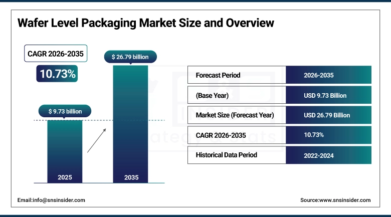
The Wafer Level Packaging Market size is valued at USD 9.73 Billion in 2025 and is projected to reach USD 26.79 Billion by 2035, growing at a CAGR of 10.73% during the forecast period 2026–2035.
The Wafer Type Packaging Market analysis report provides a detailed analysis of technology developments, process improvements, and application developments. Increasing demand for miniaturized electronics, rising use of heterogeneous devices, increasing adoption of fan-out and interposer-based packaging, and expanding semiconductor manufacturing capabilities are expected to drive strong growth in Wafer Type Packaging during 2026-2035.
Wafer type packaging shipments surpassed several billion packaged devices in 2025. The surge in demand was fuelled by smartphone manufacturing, the swift rollout of 5G networks, and the growing requirement for small, dependable semiconductor parts.
Wafer Level Packaging Market Size and Growth:
-
Market Size in 2025: USD 9.73 Billion
-
Market Size by 2035: USD 26.79 Billion
-
CAGR: 10.73% from 2026 to 2035
-
Base Year: 2025
-
Forecast Period: 2026–2035
-
Historical Data: 2022–2024
To Get more information on Wafer Level Packaging Market - Request Free Sample Report
Wafer Level Packaging Market Trends:
-
Increased use of heterogeneous devices such as logic, memory, and sensors in a single package for AI and HPC applications.
-
Increasing need for ultra-thin and ultra-lightweight packaging solutions for wearables, IoT devices, and medical devices.
-
Expansion of fan out WLP technology for automotive applications to meet increasing thermal and reliability needs.
-
Migration of redistribution layer scaling below 2µm for higher interconnect density.
-
Portability and modularity of WLP solutions for flexible and foldable devices.
-
More collaboration between foundries and OSATs for innovation in fan out and interposer technologies.
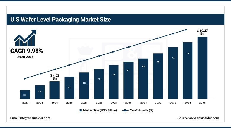
U.S. Wafer Level Packaging Market Size Outlook:
The U.S. wafer Level Packaging Market is expected to grow from its current value of 4.02 billion dollars to 10.37 billion dollars in strong growth from 2026-2035, with a CAGR of 9.98%. The market's expansion is being driven by a significant increase in the need for advanced semiconductor packages. This demand is felt across the board, impacting everything from everyday electronics to automobiles and complex computing systems.
Wafer Level Packaging Market Growth Drivers:
-
Rising demand for miniaturized and high‑performance semiconductor devices is driving adoption of advanced wafer level packaging technologies.
The increasing integration of heterogeneous components, the escalating demand for higher interconnect density, and the expanding scope for consumer electronics, automotive, and high-performance computing are the key drivers for the Wafer Level Packaging Market. Semiconductor fabrication plants and outsourced assembly services are leaning more heavily on fan-out, fan-in, and interposer approaches. These solutions offer improved efficiency, better thermal management, and increased device reliability. The adoption of these technologies is being further fuelled by advancements in redistribution layer scaling, defect detection, and sustainability initiatives, all of which contribute to better performance and market expansion.
In 2025, more than 60% of the top semiconductor fabrication facilities and outsourced assembly and test providers embraced advanced wafer-level packaging.
Wafer Level Packaging Market Restraints:
-
High complexity and cost of advanced wafer level packaging processes remain a significant barrier to widespread adoption.
Wafer Level Packaging Market is affected by complex manufacturing steps, lack of a skilled workforce, and high capital investment in advanced packaging technologies. Yield issues in fan out and interposer technologies, and difficulties in scaling down redistribution layers below 2µm, are affecting the efficiency and profitability of Wafer Level Packaging. Unfavourable reliability for automotive and high-performance computing applications, and supply chain constraints for Wafer Level Packaging materials and equipment, are affecting the Wafer Level Packaging Market.
More than 40% of semiconductor fabrication plants encountered yield and process integration issues in 2025 for implementing advanced Wafer Level Packaging technologies.
Wafer Level Packaging Market Opportunities:
-
Expanding demand for advanced packaging in AI, HPC, and 5G infrastructure is opening new growth avenues for wafer level technologies.
Wafer Level Packaging Market has opportunities arising from increasing adoption in automotive electronics, electric vehicles, and healthcare devices, where miniaturization and reliability are critical requirements. Hybrid packaging methods, such as fan-out and interposer technologies, offer new possibilities for integration, which can potentially lead to better performance.
More than 55% of leading semiconductor companies in 2025 started their R&D initiatives on next-generation wafer level packaging solutions for supporting emerging applications in computing, automotive, and medical technologies.
Wafer Level Packaging Market Segmentation Analysis:
-
By Packaging Type, Fan-in WLP (FI-WLP) held the largest market share of 42.25% in 2025, while Interposer/2.5D/3D are expected to grow at the fastest CAGR of 14.42% during 2026–2035.
-
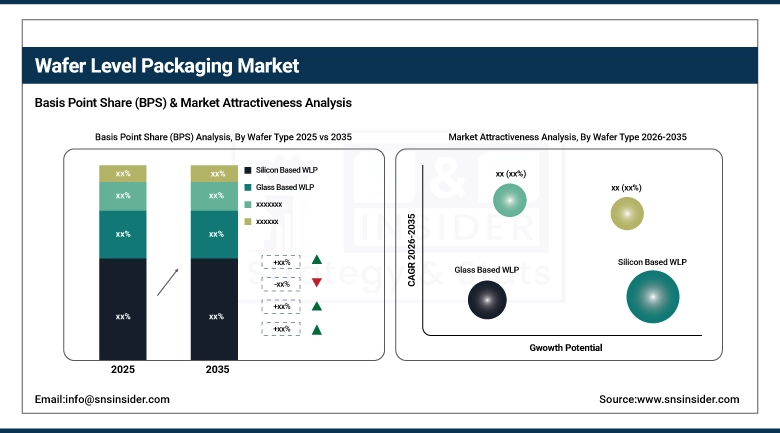
By Wafer Type, Silicon Based WLP dominated with 76.88% market share in 2025, whereas Glass Based WLP are projected to record the fastest CAGR of 12.11% through 2026–2035.
-
By Device Type, Logic ICs accounted for the highest market share of 34.45% in 2025, while Sensors are expected to grow at the fastest CAGR of 12.86% during the forecast period.
-
By End User Industry, Consumer Electronics held the largest share of 37.11% in 2025, while Automotive are expected to grow at the fastest CAGR of 15.99% during the forecast period.
By Wafer Type, Silicon based WLP Dominate While Biologics & Glass‑based WLP Grow Rapidly:
Wafer Level Packaging based on Silicon dominates the market due to the reliability of the material, its ability to be integrated into advanced nodes, and its usage in consumer products and high-performance computing. In 2025, billions of devices are packaged using silicon substrates. It is an indication of the industry's acceptance of the material due to its reliability.
Wafer Level Packaging based on Glass is the fastest-growing segment due to the material's superior insulation characteristics, reduced signal loss, and usage in RF/optical communications. It gained popularity in the next wave of devices due to the increase in the usage of next-generation 5G devices, advanced sensor technology, and the emergence of flexible electronics.
By Packaging Type, Fan‑in Wafer Level Packaging (FI‑WLP) Dominates While Interposer/2.5D/3D TSV Packaging Grow Rapidly:
The Fan in Wafer Level Packaging (FI WLP) segment dominate the share in the market due to its reliability, cost-effectiveness, and adoption in mobile and consumer electronics. In 2025, utilization crossed the billion-dollar figure in terms of packaged devices, indicating its popularity among semiconductor fabs and OSATs due to its well-established and high-yielding technology.
Interposer/2.5D/3D TSV Packaging is the fastest-growing segment of the market due to increasing demand from AI accelerators, GPUs, and HPC applications. In the past few years, there has been significant adoption of this technology, especially in advanced nodes and heterogeneous integration, including logic memory stacking and next-generation computing.
By Device Type, Logic ICs Dominate While Sensors Grow Rapidly:
Logic ICs segment dominates the largest market share due to their importance in powering high-end computing devices, mobile processors, and AI accelerators. Billions of logic devices have been packaged using WLP technologies in recent years, signifying the strong industry focus on high performance and reliability for the next generation of electronics.
Sensors hold the fastest growing market segment due to increasing demand for sensors in IoT, automotive, and health applications. There was a significant increase in the use of sensors in 2025, signifying their growing importance in creating connected and intelligent applications.
By End User Industry, Consumer Electronics Dominate While Automotive Grow Rapidly:
Consumer Electronics segment dominate the highest share in the market due to the high adoption of Wafer Level Packaging in smart phones, tablets, wearables, and other small form factor electronic products that demand high performance and miniaturization. Billions of consumer electronic products were enabled with WLP solutions in 2025, demonstrating the high reliance on advanced packaging solutions for performance, efficiency, and reliability
Automotive is the fastest-growing segment, driven by increasing adoption in ADAS, Electric Vehicle Power Systems, and Infotainment modules. Utilization of WLP solutions increased with the adoption of WLP technologies in automotive systems to satisfy stringent thermal, safety, and reliability requirements.
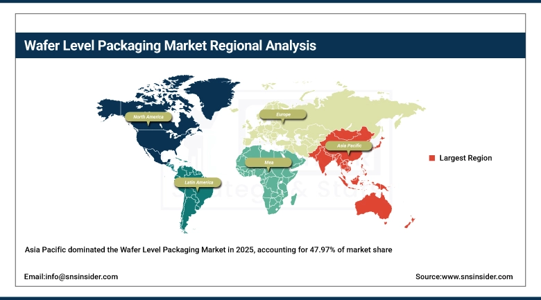
Asia‑Pacific Wafer Level Packaging Market Insights:
Asia Pacific Wafer Level Packaging Market dominated the market share at 47.97%, driven by strong semiconductor manufacturing bases in countries such as Taiwan, South Korea, Japan, and China. This market grows due to increasing consumer electronics demand, rapid deployment of 5G technologies, and increasing automotive and artificial intelligence-related applications. High penetration of fan in and fan out WLP technologies, along with significant investment in advanced packaging technologies, helps Asia Pacific dominate the market. Continuous advancements in redistribution layer scaling, heterogeneous integration, and sustainability practices help Asia Pacific dominate the global wafer level packaging technologies market.
Get Customized Report as per Your Business Requirement - Enquiry Now
China Wafer Level Packaging Market Insights:
The China Wafer Level Packaging Market is driven by strong domestic semiconductor demand, government initiatives in achieving self-sufficiency, and the rapid growth of OSATs such as JCET. Growing demand in smartphones, electric vehicles, and AI accelerators is boosting the adoption of fan out and 2.5D/3D solutions. Strategic investments in advanced fabs, partnerships with global technology leaders, and advancements in glass-based substrates and hybrid solutions strengthen China’s position in the Asia Pacific region.
North America Wafer Level Packaging Market Insights:
The North America Wafer Level Packaging Market has been Fastest growing with a CAGR of 11.95%, driven by the strong semiconductor manufacturing industry base available in the region, covering the U.S. and Canadian markets. This growth is fuelled by the increasing demand for advanced packaging solutions for consumer electronics, automotive, and high-performance computing applications. Additionally, the increasing adoption of fan-in and fan-out WLP technologies and investment in 2.5D/3D integration activities have cemented the region’s strong position for the mature Wafer Level Packaging market.
U.S. Wafer Level Packaging Market Insights:
The US Wafer Level Packaging Market is driven by strong demand for semiconductors, high adoption of fan out and interposer solutions, and strong investments in domestic fabs. Growing demand from AI accelerator, 5G infrastructure, and automotive electronics segments adds to the growth story. Expanding advanced packaging infrastructure, partnerships between OSATs and foundries, and advancements in hybrid solutions make the US the largest Wafer Level Packaging Market in North America.
Europe Wafer Level Packaging Market Insights:
The Europe Wafer Level Packaging Market has a strong focus on research, sustainability, and engineering standards. Growth in the Europe Wafer Level Packaging Market is driven by increasing demand for miniaturized electronics in industrial automation, medical equipment, and automotive safety systems. Companies in Europe are focusing on eco-friendly packaging solutions, green fabs, and WLP in new application areas such as smart manufacturing and renewable energy systems. Joint R&D initiatives in Germany, France, and the Netherlands are adding strength to the Europe Wafer Level Packaging Market.
Germany Wafer Level Packaging Market Insights:
The Germany Wafer Level Packaging Market is fuelled by its dominance in the automotive electronics, industrial IoT, and precision engineering sectors. German companies are increasingly adopting Wafer Level Packaging technology for advanced driver assistance systems (ADAS), power modules for electric vehicles, and smart factory sensors. The German government is providing strong support for semiconductor innovation, coupled with academia-industry collaborations, to accelerate innovation in glass-based substrates and hybrid packaging.
Latin America Wafer Level Packaging Market Insights:
The Latin America Wafer Level Packaging Market is in its development stage and is being fuelled by the increasing electronics manufacturing base in Brazil and Mexico. In addition, the increasing need for consumer electronics and automotive electronics is providing a boost to the market. There is a gradual increase in the use of fan in and fan out WLP technologies in the region, and local players are investing in advanced semiconductor manufacturing plants.
Middle East & Africa Wafer Level Packaging Market Insights:
The Middle East & Africa Wafer Level Packaging Market is in its infancy stage. However, the market is expected to have immense growth potential due to the increase in the development of telecom infrastructure, smart city initiatives, and the rising need for automotive and industrial electronics. The UAE and South Africa are developing advanced technology hubs, thereby boosting the adoption of miniaturized semiconductor devices. In addition, the rising interest in renewable energy systems and medical devices is also providing an opportunity for the integration of Wafer Level Packaging.
Wafer Level Packaging Market Competitive Landscape:
Jiangsu Changjiang Electronics Technology Co. JCET, a major Chinese player in semiconductor packaging and testing, is known for its leadership in advanced packaging. This includes wafer level packaging, system-in-package, and 2.5D/3D integration. JCET's considerable manufacturing prowess, combined with its robust connections across the Asia-Pacific, positions it as a significant force in advancing miniaturization and high-performance chip designs.
-
In 2025, JCET expanded its advanced packaging facility in Jiangyin, China, enhancing production capacity for fan-out WLP to meet rising demand in 5G and automotive electronics.
Taiwan Semiconductor Manufacturing Company Limited (TSMC) reigns as the globe's leading semiconductor foundry, and it's a key player in wafer level packaging. TSMC integrates WLP into its cutting-edge manufacturing processes, offering solutions such as InFO (Integrated Fan-Out) packaging. This method delivers improved performance, a more compact design, and superior thermal management.
-
In 2025, TSMC introduced next-generation InFO technology optimized for AI accelerators, enabling higher bandwidth and improved power efficiency in advanced computing systems.
Amkor Technology, Inc., a US-based OSAT firm, excels in advanced packaging. Its capabilities span wafer level packaging, fan-out, and flip-chip technologies. The company caters to a worldwide clientele, including those in consumer electronics, automotive, and networking sectors, drawing on its proficiency in high-volume manufacturing and dependability. Amkor's strategic emphasis on fan-out wafer level packaging and system-in-package solutions has solidified its standing as a crucial supplier to prominent semiconductor companies globally.
-
In 2025, Amkor announced the expansion of its advanced packaging operations in Korea, increasing capacity for fan-out WLP to support demand from smartphone and automotive semiconductor markets.
Wafer Level Packaging Companies are:
-
Jiangsu Changjiang Electronics Technology Co. Ltd.
-
Taiwan Semiconductor Manufacturing Company Limited (TSMC)
-
ASE Group (Advanced Semiconductor Engineering, Inc.)
-
Lam Research Corporation
-
ASML Holding N.V.
-
Qualcomm Technologies, Inc.
-
KLA Corporation
-
Deca Technologies
-
Nordson Corporation
-
ECI Technology
-
CAPLINQ Corporation
-
Nepes Corporation
-
SUSS MicroTec SE
-
Brewer Science, Inc.
-
Tokyo Electron Limited (TEL)
-
Samsung Electronics Co., Ltd.
-
Intel Corporation
-
STATS ChipPAC Pvt. Ltd.
| Report Attributes | Details |
|---|---|
| Market Size in 2025 | USD 9.73 Billion |
| Market Size by 2035 | USD 26.79 Billion |
| CAGR | CAGR of 10.73% From 2026 to 2033 |
| Base Year | 2025 |
| Forecast Period | 2026-2035 |
| Historical Data | 2022-2024 |
| Report Scope & Coverage | Market Size, Segments Analysis, Competitive Landscape, Regional Analysis, DROC & SWOT Analysis, Forecast Outlook |
| Key Segments | • By Packaging Type (Fan-in WLP (FI-WLP), Fan-out WLP (FO-WLP), Interposer/2.5D/3D TS, Others) • By Wafer Type (Silicon Based WLP, Glass Based WLP, Organic Substrates, Others) • By Device Type (Logic ICs, Memory ICs, RF & Analog ICs, Others) • By Patient Type (Adults, Geriatrics, Paediatrics, Others) • By End User Industry (Consumer Electronics, Automotive, IT & Telecom, Industrial/IoT, Others) |
| Regional Analysis/Coverage | North America (US, Canada), Europe (Germany, UK, France, Italy, Spain, Russia, Poland, Rest of Europe), Asia Pacific (China, India, Japan, South Korea, Australia, ASEAN Countries, Rest of Asia Pacific), Middle East & Africa (UAE, Saudi Arabia, Qatar, South Africa, Rest of Middle East & Africa), Latin America (Brazil, Argentina, Mexico, Colombia, Rest of Latin America). |
| Company Profiles | Jiangsu Changjiang Electronics Technology Co. Ltd.,Taiwan Semiconductor Manufacturing Company Limited (TSMC),Amkor Technology, Inc., ASE Group (Advanced Semiconductor Engineering, Inc.),Lam Research Corporation,ASML Holding N.V.,Qualcomm Technologies, Inc.,Applied Materials, Inc.,KLA Corporation,Deca Technologies,Nordson Corporation,ECI Technology, CAPLINQ Corporation, Nepes Corporation, SUSS MicroTec SE, Brewer Science, Inc., Tokyo Electron Limited (TEL), Samsung Electronics Co. Ltd.,Intel Corporation, STATS ChipPAC Pte. Ltd. |
Frequently Asked Questions
Consumer electronics remain the largest demand driver, while automotive electronics are the fastest‑growing, fuelled by ADAS, EV power systems, and infotainment modules requiring reliable, high‑density packaging.
Glass‑based WLP offers opportunities in RF, optical communication, and 5G infrastructure due to superior electrical insulation, lower signal loss, and suitability for high‑frequency applications.
Logic ICs lead the market with market size of 34.45%, as they are essential for powering advanced processors, AI accelerators, and next‑generation computing systems, making them the most widely packaged devices.
Interposer/2.5D/3D packaging is rapidly expanding because of its ability to integrate logic and memory for AI, HPC, and GPU applications, enabling higher performance and heterogeneous integration.
Fan‑in WLP dominates with market share of 42.25% due to its cost‑effectiveness, proven reliability, and widespread adoption in mobile and consumer electronics, where compact designs and high yields are critical.
Get in Touch
