Semiconductor Packaging Materials Market Report Scope & Overview:
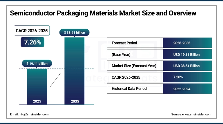
The Semiconductor Packaging Materials Market size was valued at USD 19.11Billion in 2025 and is projected to reach USD 38.51Billion by 2035, growing at a CAGR of 7.26% during 2026–2035.
High demand for high-performance, reliable, and miniaturized electronic devices in sectors such as consumer electronics, automotive, telecommunications, and healthcare is driving the growth of Semiconductor Packaging Materials market. Organic substrates, ceramic packages, bonding wires and thermal management compounds are key materials that improve chip efficiency and lifetime. Innovations in 3DIC, Cu-Cu bonding and high density interposers continue to push the packaging envelope. This market growth is further bolstered by the rising adoption of AI, electric vehicles, smart devices, which will drive technological development as well as global supply chain.
In March 2026, Niching Industrial Corp. reported strong early revenue growth, driven by AI-driven thermal products that enhance semiconductor packaging and testing efficiency. The company achieved NT USD 200 million in January February, reflecting rising demand for advanced cooling solutions in high-performance computing and next-generation chip applications.
Semiconductor Packaging Materials Market Size and Forecast:
-
Market Size in 2025: USD 19.11 Billion
-
Market Size by 2035: USD 38.51 Billion
-
CAGR: 7.26% during 2026–2035
-
Base Year: 2025
-
Forecast Period: 2026–2035
-
Historical Data: 2022–2024
To Get more information on Semiconductor Packaging Materials Market - Request Free Sample Report
Semiconductor Packaging Materials Market Highlights:
-
Organic substrates and ceramic packages dominate the product landscape, supporting advanced chip performance.
-
Expansion of 3DIC, EMIB, and CoWoS technologies boosts adoption of specialized packaging materials.
-
North America and Asia-Pacific lead market development due to strong semiconductor manufacturing infrastructure.
-
Automotive, healthcare, and communication sectors are emerging as key end users of advanced packaging materials.
-
Increasing focus on thermal management, adhesion, and protection materials enhances reliability and efficiency of semiconductor devices.
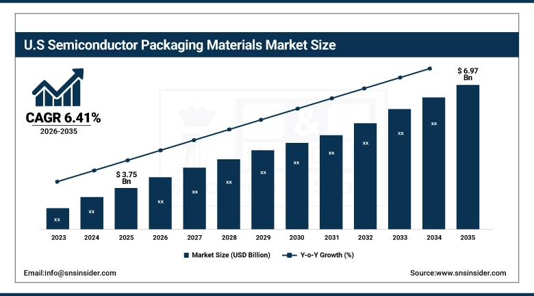
U.S. Semiconductor Packaging Materials Market Size Outlook:
The U.S. Semiconductor Packaging Materials Market was valued at USD 3.75 Billion in 2025 and is projected to reach USD 6.97 Billion by 2035, growing at a CAGR of 6.41% during 2026–2035, growth for the market is attributed to the rise in demand for advanced electronics, high-performance computing, and AI-enabled devices. The innovation in semiconductor packaging is driven by important materials like organic substrates, ceramic packages, bonding wires and thermal management compounds. This is further propelled by increase in uptake of electric vehicles, development of 5G technology, and adoption of smart devices. Moreover, government strategies encouraging domestic semiconductor manufacturing—along with the growth of advanced packaging such as 3DIC and high-density emerging interposers are expanding production capacity and supply chain flexibility, establishing the U.S. as a major player in the global semiconductor packaging ecosystem.
Semiconductor Packaging Materials Market Drivers:
-
Rising Demand for Advanced Applications Drives Semiconductor Packaging Market
The growing adoption of AI, high-performance computing, 5G, and automotive electronics is driven by increasing adoption of AI, high-performance computing, 5G and automotive electronics. More complex devices, particularly the hybrid and half-IC packaged ones, are providing significant drive toward advanced materials – specifically ceramic packages, adhesives, thermal management, etc. for miniaturized & high-density assembly and processing efficiency. Such demand for application requirements in turn directly impacts R&D investments, facilitates next-generation packaging technologies and accentuates the demand for proven high-performance interconnects. As a result, the global demand drives broadening scope for growth, innovation and competition within semiconductor packaging firms, yearning to provide cost-effective, reliable, state-of-the-art semiconductor packaging solutions to work in perfect unison worldwide.
In Dec 2025, City University of Hong Kong pioneer s breakthrough 3DIC semiconductor packaging materials with patented chemical additives for copper electroplating, enhancing chip performance and reliability; research funded under RAISe+ Scheme.
Semiconductor Packaging Materials Market Restraints:
-
Impact of Cost, Complexity, and Regulations on Semiconductor Packaging Growth
The high production price combined with high scalability hurdles and lengthy time-to-market of advanced materials like ceramic packages, adhesives, and thermal management solutions is a bottleneck. Relying on very specific raw materials for low-volume applications (including CFC-free and green polyurethanes) and possible supply chain shortages further complicate and prolong the production lead time. The pace of technological development requires constant investment in research and development while intense environmental regulations limit material choice and fate. In conjunction, these aspects limit adoption, increase operational complexities, and impact competitive dynamics and slow down the market growth trajectory of semiconductor packaging materials partially in light of the increasing demand of electronic devices to become increasingly providing ever-higher performance while being miniature.
Semiconductor Packaging Materials Market Opportunities:
-
Emerging Opportunities in Advanced Semiconductor Packaging
The semiconductor packaging materials market presents significant growth in the coming years, as the demand for many high-performance, AI-enabled, and automotive electronics is on the rise. Developments in packaging solutions especially high density integration, miniaturization and reliable thermal management are paving the way for creating new opportunities. Players can develop differentiated and specialized materials such as advanced adhesives, advanced ceramic packages, and encapsulation materials to meet the evolving needs of the industry. This boost in efficiency, performance, and reliability are only going to play further into designing solutions which can be for more complex semiconductor devices, allowing stakeholders an important prospect to take benefit of the transition to next-generation semiconductor packaging and secure a competitive position in the growing global ecosystem.
In Sept 2025, JX Advanced Metals Became Member of Consortium JOINT3 for Next-generation Semiconductor Packaging on Accelerating Innovation for Advanced Packaging Material with Global Industry Leaders.
Semiconductor Packaging Materials Market Segment Highlights:
-
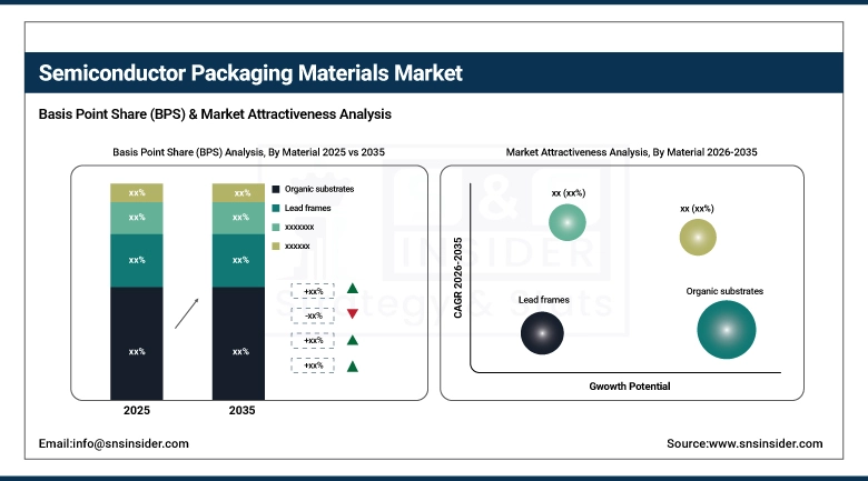
By Material: Dominant – Organic substrates (44.70% → 42.30%, CAGR 6.67%); Fastest-Growing – Ceramic packages (15.70% → 21.30%, CAGR 10.53%)
-
By Technology: Dominant – Grid Array (25.20% → 26.80%, CAGR 7.92%); Fastest-Growing – Others (10.10% → 10.90%, CAGR 8.08%)
-
By End Use: Dominant – Consumer Electronics (34.50% → 30.50%, CAGR 5.94%); Fastest-Growing – Automotive (15.50% → 19.50%, CAGR 9.72%)
-
By Application: Dominant – Thermal Management Materials (25.30% → 27.70%, CAGR 8.23%); Fastest-Growing – Adhesives & Underfills (10.20% → 11.80%, CAGR 8.82%)
By Material: Organic Substrates Dominant; Ceramic Packages Fastest-Growing
Organic substrates are the dominant material segment in the global semiconductor packaging materials market due to their cost-effectiveness, ease of manufacturing, and widespread use in consumer electronics and communication devices. Ceramic packages are the fastest-growing segment, driven by increasing demand for high-performance, high-reliability applications in automotive, aerospace, and advanced computing technologies.
By Technology: Grid Array Dominant; Others Technology Segment Fastest-Growing
Grid Array is the dominant technology segment in the global semiconductor packaging materials market due to its high-density design, reliability, and widespread adoption across consumer electronics and communication devices. The Others technology segment is the fastest-growing, owing to the growing demand for high-performance, high-reliability applications such as automotive, aerospace and advanced computing technologies.
By End Use: Consumer Electronics Dominant; Automotive End-Use Fastest-Growing
Consumer electronics is the dominant end-use segment in the global semiconductor packaging materials market due to mass adoption, large production volumes, and consistent demand for smartphones, laptops, and wearable devices. The automotive market is growing the fastest as increased electronic content in cars, electric vehicle (EV) adoption, and advanced driver-assistance systems (ADAS) demand high-reliability semiconductor packaging.
By Application: Thermal Management Materials Dominant; Adhesives & Underfills Application Fastest-Growing
Thermal management materials are the dominant application segment in the global semiconductor packaging materials market due to their critical role in heat dissipation and reliability of high-performance chips. Intelligent process control is predicted to lead the market for electronics underfill and encapsulation materials throughout the forecast period Propelled by growing demand in advanced packaging, AI chips, automotive electronics, and next-generation semiconductor devices, adhesives & underfills have become the fastest growing application segment.
Semiconductor Packaging Materials Market Regional Highlights:
-
North America: 29.80% (2025) → 28.20% (2035), Dominant Region with strong semiconductor manufacturing infrastructure, advanced R&D facilities, and high adoption of AI and high-performance computing chips (CAGR 2.04%)
-
Europe: 19.80% (2025) → 18.20% (2035), Moderate Growth Region driven by automotive, industrial electronics, and government incentives for advanced semiconductor packaging technologies (CAGR 2.04%)
-
Asia-Pacific: 35.50% (2025) → 39.50% (2035), Fastest-Growing Region fueled by China, Japan, South Korea, and Taiwan’s electronics hubs, high demand for advanced packaging, and AI-driven semiconductor adoption (CAGR 3.80%)
-
South America: 5.00% (2025) → 5.00% (2035), Steady Growth Region supported by rising consumer electronics, automotive applications, and gradual expansion of semiconductor assembly facilities (CAGR 3.90%)
-
Middle East & Africa: 9.90% (2025) → 9.10% (2035), Emerging Growth Region driven by UAE, Saudi Arabia, and South Africa investing in semiconductor assembly, testing facilities, and advanced packaging technologies (CAGR 3.05%)
Asia-Pacific Semiconductor Packaging Materials Market Insights:
Asia-Pacific region dominates the market share across the world, due to the presence of major electronics manufacturing hubs such as China, Japan, South Korea, and Taiwan. High demand for advanced packaging, high-density substrates, and AI chips drives revenue, with extensive semiconductor supply chains, government incentives, and rapid transition to the next generation of technologies for consumer electronics, automotive, and container applications propelling growth.
Get Customized Report as per Your Business Requirement - Enquiry Now
China Semiconductor Packaging Materials Market Insights:
The Semiconductor Packaging Materials market is predominantly held by China, who takes the largest share of the Semiconductor Packaging Materials both in terms of production and consumption, due to its high electronics manufacturing base, government policies supporting growth, and increased number of in-house packaging technology adaptions.
North America Semiconductor Packaging Materials Market Insights:
The North America Semiconductor Packaging Materials market is experiencing robust growth, driven by increasing demand for advanced semiconductor packaging in AI, high-performance computing, and automotive electronics. Key drivers include significant investments in domestic chip manufacturing, government incentives under initiatives like the CHIPS Act, adoption of heterogeneous integration technologies, and rising need for high-reliability materials to support next-generation packaging solutions in servers, data centers, and consumer electronics.
United States Semiconductor Packaging Materials Market Insights:
The United States Semiconductor Packaging Materials market is growing steadily, propelled by strong interest in chip packaging technologies - especially for applications in AI, high performance computing, and automotive electronics, along with localized chip manufacturing investment and enablement-focused government programs.
Europe Semiconductor Packaging Materials Market Insights:
Europe Semiconductor Packaging Materials Market is currently growing moderately, driven by some exemplary automotive, industrial and consumer electronics and so forth. It is being propelled by the push from the government for semiconductor manufacturing, the increasing requirement for high-performance computing and AI applications, and investments from leading companies in domestic production and research and development (R&D) facilities. The steady growth of the market in the region is further prompted due to the European region being highly inclined towards sustainable and high-reliability packaging materials.
Germany Semiconductor Packaging Materials Market Insights:
The Germany Semiconductor Packaging Materials market is expanding steadily, driven by strong automotive and industrial electronics demand, adoption of advanced packaging technologies, and strategic investments in local semiconductor manufacturing and R&D facilities.
Latin America Semiconductor Packaging Materials Market Insights:
The Latin America Semiconductor Packaging Materials market is witnessing steady growth, due to rise in end-user industries, such as consumer electronics, automotive, and industrial. The growth in the market is driven by the increase in foreign investments, increasing local semiconductor assembly and testing facilities, government initiatives to strengthen the electronics manufacturing ecosystem, and increasing adoption of advance packaging technologies to provide performance and reliability specifications in next-generation devices across the region.
Brazil Semiconductor Packaging Materials Market Insights:
Brazil leads the Latin America Semiconductor Packaging Materials market, Driven by strong electronics manufacturing base in the country, with growing automotive and consumer electronics sectors, and favourable government initiatives.
Middle East & Africa (MEA) Semiconductor Packaging Materials Market Insights:
The Middle East & Africa Semiconductor Packaging Materials market is gradually expanding, fueled by increasing demand for consumer electronics, automotive, and industrial applications. This growth is driven by increasing investments in local semiconductor assembly and testing facilities, government efforts to nurture high-tech manufacturing ecosystems and higher adoption of advanced packaging technologies. By doing so, countries like the UAE, Saudi Arabia and South Africa have positioned themselves as new poles of appeal, luring in international partnerships and tech and shifting them closer to regional semiconductor supply chains and the increasing needs of the sector.
United Arab Emirates Semiconductor Packaging Materials Market Insights:
The United Arab Emirates (UAE) is the dominant country, due to its infrastructure for electronics manufacturing, as well as various strategic investments and government policies aimed at industrial development in high-tech and setting up a semiconductor ecosystem.
Semiconductor Packaging Materials Market Competitive Landscape:
DuPont, formally E. I. du Pont de Nemours & Co., is an American multinational chemical and materials company founded in 1802 by French‑born Éleuthère Irénée du Pont in Wilmington, Delaware; over more than two centuries it has evolved from a gunpowder mill into a global leader in advanced chemicals, polymers, and specialty materials serving electronics, industrial, agriculture, and safety markets.
-
In March 2026, DuPont spun off Qnity, which opened a 385,000‑sq‑ft semiconductor manufacturing facility in Delaware to produce CMP pads for advanced AI and high-performance chips, strengthening domestic operations and supply chain resilience.
Samsung Electro‑Mechanics, established in 1973, is a South Korean multinational company specializing in electronic components, including multilayer ceramic capacitors, camera modules, and advanced semiconductor packaging materials. The company focuses on high-performance computing, AI-driven electronics, and next-generation package substrates, leveraging global R&D and manufacturing capabilities.
-
In Nov 2025, Samsung Electro‑Mechanics signed an MOU with Sumitomo Chemical Group to establish a joint venture for manufacturing ‘Glass Core,’ a key material for next-generation semiconductor package substrates, aiming to lead the advanced substrate market amid rising AI and high-performance computing demand.
Semiconductor Packaging Materials Companies are:
-
BASF SE
-
Henkel AG & Co. KGaA
-
Hitachi Ltd.
-
Kyocera Corporation
-
LG Innotek
-
Shin‑Etsu Chemical Co., Ltd.
-
Sumitomo Chemical / Sumitomo Bakelite
-
Tanaka Kikinzoku Group
-
Toppan Printing Co., Ltd.
-
Nippon Micrometal Corporation
-
Alpha Advanced Materials
-
Heraeus Electronics
-
Indium Corporation
-
ChipMOS Technologies Inc.
-
Powertech Technology Inc.
-
Unimicron Technology Corporation
-
Samsung Electronics Co., Ltd.
-
Texas Instruments Inc.
| Report Attributes | Details |
|---|---|
| Market Size in 2025 | USD 19.11 Billion |
| Market Size by 2035 | USD 38.51 Billion |
| CAGR | CAGR of 7.26% From 2026 to 2035 |
| Base Year | 2025 |
| Forecast Period | 2026-2035 |
| Historical Data | 2022-2024 |
| Report Scope & Coverage | Market Size, Segments Analysis, Competitive Landscape, Regional Analysis, DROC & SWOT Analysis, Forecast Outlook |
| Key Segments | • By Material (Automatic layer deposition, Chemical vapor diposition, Etching, Oxidation and Others) • By Technology (Foundry, Memory and Integrated device manufacturer) • By End Use(300 mm wafer size, 200 mm wafer size and 150 mm wafer size) • By Application (Node size between 14nm and 28nm, Node size between 6nm and 14nm, Node size more than 28nm, Node size between 5nm and 6nm and Node size below 5nm) |
| Regional Analysis/Coverage | North America (US, Canada), Europe (Germany, UK, France, Italy, Spain, Russia, Poland, Rest of Europe), Asia Pacific (China, India, Japan, South Korea, Australia, ASEAN Countries, Rest of Asia Pacific), Middle East & Africa (UAE, Saudi Arabia, Qatar, South Africa, Rest of Middle East & Africa), Latin America (Brazil, Argentina, Mexico, Colombia, Rest of Latin America). |
| Company Profiles | Key players in the Semiconductor Packaging Materials Market include DuPont, BASF SE, Henkel AG & Co. KGaA, Hitachi Chemical, Kyocera Corporation, LG Innotek, Shin‑Etsu Chemical, Sumitomo Chemical, Toray Industries, Tanaka Kikinzoku, Toppan Printing, Nippon Micrometal, Alpha Advanced Materials, Heraeus Electronics, Indium Corporation, ChipMOS Technologies, Powertech Technology, Unimicron Technology, Samsung Electronics, and Texas Instruments. |
Get in Touch
