3D Semiconductor Packaging Market Size Analysis:
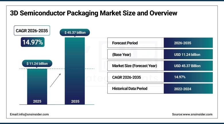
The 3D Semiconductor Packaging Market was valued at USD 11.24 Billion in 2025 and is projected to grow at 14.97% CAGR to reach USD 45.37 Billion by 2035.
The 3D Semiconductor Packaging Market is expanding due to the high-performance electronics is driving the growth of the 3D semiconductor packaging market. Progression of 3D ICs, FOWLP, and System-in-Package technologies offer a higher level of integration and functionality. AI, IoT, automotive electronics, HPC applications are promoting the advanced packaging adoption. Growing emphasis on energy efficiency, reliability, and environment-friendly materials would continue to fuel market growth.
Automotive electronics (ADAS, EVs, zonal architectures) contributed 17% of 3D packaging adoption in 2024, a 30% YoY increase due to higher compute requirements.
Market Size and Growth Projection:
-
Market Size in 2025 USD 11.24 Billion
-
Market Size by 2035 USD 45.37 Billion
-
CAGR of 14.97% From 2026 to 2035
-
Base Year 2025
-
Forecast Period 2026-2035
-
Historical Data 2022-2024
To Get More Information On 3D Semiconductor Packaging Market - Request Free Sample Report
3D Semiconductor Packaging Market Trends
-
Increasing demand for small sized chips with high efficiency in the AI accelerator, automotive, and mobile devices.
-
5G networks, IOT devices and cloud computing are driving packaging needs.
-
Meanwhile, incresingly environment-friendly, energy-saving, and high-integration package are being desingned by our companies.
-
Introduction of TSV, FOWLP, and advanced interconnects enhance performance and device functionality.
-
Collaborations help technology acceleration and improve time-to-market for new semiconductor devices.
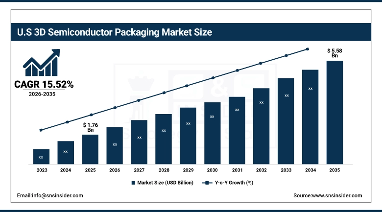
U.S. 3D Semiconductor Packaging Market Size Outlook
The U.S. 3D Semiconductor Packaging Market size was valued at USD 1.76 Billion in 2025 and is projected to reach USD 5.58 Billion by 2035, growing at a CAGR of 15.52% during 2026-2035. 3D Semiconductor Packaging Market growth is driven by rising the demand for high-performance computing and AI enabled devices coupled with rise in penetration of Through-Silicon Via (TSV), FOWLP, and advanced interconnect technologies leading higher density and miniaturization. Growth of mobile devices, automotive electronics, and IoT applications drives adoption in various industries, and investment in semicon fabrication and packaging by leading domestic players increases production capacity.
The 3D Semiconductor Packaging Market trends include the trong e-commerce and cloud computing growth further fuels the need for top-performance, scalable semiconductor solutions and these partnerships between fabless companies and OSATs support furthering innovation and speed to market of 3D packaging technologies.
3D Semiconductor Packaging Market Growth Drivers:
-
Rising Demand for High-Performance, Miniaturized Electronics and AI-Enabled Devices.
Growth of the 3D semiconductor packaging market is driven by high demand for high-density and small electronic devices. AI, IoT, HPC, automotive and mobile growth attracts advanced packaging. Advances in TSV, FOWLP, and interconnect technologies enable greater speed, energy efficiency, and device capabilities. Power-efficient, reliable and scalable technologies to address changing market needs are main R&D targets for manufacturers.
AI and HPC workloads now account for 45% of all advanced packaging demand, with nearly 100% adoption of 3D-stacked memory (HBM3/HBM3E) in AI accelerators from NVIDIA, AMD, and custom silicon (e.g., Google TPU, Apple M-series).
3D Semiconductor Packaging Market Restraints:
-
High Manufacturing Complexity and Cost Challenges Limiting Widespread Adoption of 3D Packaging Solutions
3D integration solutions depend on accurate alignment, custom materials, and intricate fabrication. Adoption is limited by high equipment and operational costs, which make it unfeasible for small and medium-sized manufacturers in particular. Technical issues, such as thermal, warpage and interconnect reliability, also affect yield in production. High quality and reliability as well as very high compliance makes investments and operational load even higher.
3D Semiconductor Packaging Market Opportunities:
-
Growing Adoption in Automotive, AI, IoT, and Edge Computing Applications Driving Market Expansion
Increasing need for miniaturized high performance chips in AI accelerators and automotive electronics provides opportunities. 5G, cloud, and IoT devices drive advanced packaging demand. All in all, it provides a chance of innovation due to concentration in environment-friendly, energy-saving and high-integration packaging. However, in the case of fabless identification and OSATs working together, the time to market for any products as well as technology improvement deployment is greatly enhanced.
Over 60% of AI accelerator chips launched in 2024 use advanced packaging technologies such as chiplets, Foveros (Intel), or CoWoS (TSMC), to achieve higher bandwidth and energy efficiency.
3D Semiconductor Packaging Market Segment Analysis
-
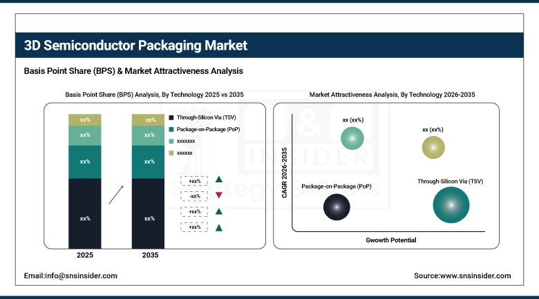
By Technology was led by Through-Silicon Via (TSV) with around 36.43% share, while Fan-Out Wafer Level Packaging (FOWLP) emerged as the fastest-growing segment with a CAGR of 15.55%.
-
By Packaging Type, Chip-Stacking dominated with nearly 56.32% share in 2025, whereas System-in-Package (SiP) is expected to grow the fastest at a CAGR of 15.58%.
-
By Application, automotive accounted for about 38.43% share in 2025, while healthcare is projected to expand at the highest pace with a CAGR of 15.64%.
-
By End-User, automotive led the market with around 38.67% share in 2025, while healthcare is anticipated to register the fastest growth at a CAGR of 15.66%.
By Technology, Through-Silicon Via (TSV) Leads Market While Fan-Out Wafer Level Packaging (FOWLP) Registers Fastest Growth
On the basis of technology, TSV (Through-Silicon Via) is estimated to account for the largest share of the 3D semiconductor packaging market in 2025. Fan-Out Wafer Level Packaging (FOWLP) is the fastest growing category, with high density and miniaturization requirements propelling its growth. Advanced interconnects and vertical stacking add performance and integration. Rising implementation across AI, automotive, and high-performance computing also speeds up the adoption of FOWLP.
By Packaging Type, Chip-Stacking Dominate While System-in-Package (SiP) Shows Rapid Growth
Chip-stacking is a leading segment in 3D semiconductor packaging market in 2025. System-in-Package (SiP) is expanding explosively due to its demand for convergence and miniaturization, and to satisfy demand for compact and high performance. Advanced stacking and integration techniques, which increase the density and capability of the device. The increasing penetration of automotive, AI and mobile applications also promotes the adoption of SiP.
By Application, Automotive Lead While Healthcare Registers Fastest Growth
Automotive is still the most advanced application for semicon packaging, fueled by increasingly complicated vehicles. The growing market for electric vehicles, advanced driver assistance systems (ADAS) and connected car applications is driving the need for high performance, compact, reliable chips to function in harsh environments. Simultaneously, and in order to fulfill the demand of miniaturized, energy-efficient electronics systems for medical devices applications the healthcare sector is rising as the one growing faster.
By End-Use, Automotive Lead While Healthcare Grow Fastest
Automotive is still the largest end user in the 3D semiconductor packaging market, due to the growing complexity of today's automobiles. This dominance is underpinned by performance chips for EVs, ADAS and connected car technologies. At the same time, health care is projected to become the fastest growing end-use segment, driven by miniaturization and energy-efficient medical devices. Advanced packaging technologies are being increasingly adopted underpinned by wearable, implantable and hand-held diagnostic devices.
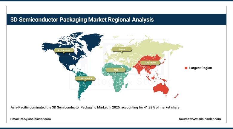
Asia-pacific 3D Semiconductor Packaging Market Insights
In 2025 Asia-Pacific dominated the 3D Semiconductor Packaging Market and accounted for 41.32% of revenue share, this leadership is due to the high concentration of semiconductor manufacturers and advanced packaging industries in the area. Demand from electronics, automobile and telecommunication industries fuels market growth. Role of favorable government policies and sustained R&D funding keep the regional market in good place.
Get Customized Report as Per Your Business Requirement - Enquiry Now
China 3D Semiconductor Packaging Market Insights
China's 3D semiconductor packaging market is growing rapidly due to increased need for advanced electronics and AI applications. There is a lot of innovation happening in market, with flip-chip and embedded die technologies leading the way. National producers are spending a lot of money on R&D for performance improvement and cost reduction.
North America 3D Semiconductor Packaging Market Insights
North America is expected to witness the fastest growth in the 3D Semiconductor Packaging Market over 2026-2035, with a projected CAGR of 15.75% due to technological innovation in areas such as consumer electronics, automotive and telecommunications. High Investments by Big Players and Governmental Projects in Advanced Packaging Technologies
U.S. 3D Semiconductor Packaging Market Insights
The U.S. market for 3D SiP is expanding rapidly as AI, IoT, and consumer electronics are progressing in the country. Such a trend is leading companies like TSMC and SK Hynix to pour billions of dollars into advanced packaging techniques including TSV and CoWoS as demand for high-performance chips go up.
Europe 3D Semiconductor Packaging Market Insights
In 2025, Europe emerged as a promising region in the 3D Semiconductor Packaging Market, due to convergence of technologies, and strategic investments and infrastructure from the market layers. Germany, in particular, has served as a center for automotive-grade semiconductor packaging work around applications including Advanced Driver Assistance Systems (ADAS) via to Electric Vehicle (EV) controllers.
Germany 3D Semiconductor Packaging Market Insights
Germany has been a large participant in the 3D semiconductor packaging market owing to its strong automotive and industrial sectors. The country's focus on advanced packaging technologies, including flip-chip and embedded-die also helps in the development of high-performance chips for applications such as electric vehicles and industrial automation.
Latin America (LATAM) and Middle East & Africa (MEA) 3D Semiconductor Packaging Market Insights
The 3D Semiconductor Packaging Market is experiencing moderate growth in the Latin America (LATAM) and Middle East & Africa (MEA) regions, due to the increased usage of advanced electronics and digital infrastructure. Growing adoption in telecommunication, automobile and consumer electronics industries is propelling the market growth. Local production investments and tech partnerships are aiding these regions in stepping up as manufacturers of semiconductors. These steps continue the momentum in which LATAM and MEA have a growing stake in worldwide 3D semiconductor packaging.
3D Semiconductor Packaging Market Competitive Landscape
Intel Corporation is the world's largest supplier of 3D semiconductor packaging technologies, including breakthrough 3D packaging innovations, such as Foveros and EMIB (Embedded Multi-die Interconnect Bridge). The company is invested in increasing their chip performance, energy efficiency, and form factors within everywhere from high performance computing to artificial intelligence and data centers.
-
In April 2024, Intel launched its next-generation Foveros Direct 3D packaging technology in volume production for its Intel 18A process node, enabling true atomic-level bonding between chiplets. This advancement allows for sub-micron interconnect pitches and significantly higher bandwidth density, positioning Intel at the forefront of 3D heterogeneous integration.
Samsung’s packaging leadership reinforces its global standing in the semiconductor business. 3D semiconductor packaging technology and High Bandwidth Memory (HBM) and Hybrid Bonding developed by Samsung are the required technology for advanced applications such as high-performance computing and AI. The company concentrates on enhancing chip density, interconnect efficiency and power performance.
-
In June 2024, Samsung announced the mass production of HBM3E (High Bandwidth Memory 3 Extended) with 12-layer stacked DRAM dies, achieving a data transfer rate of up to 9.6 Gbps. This makes it one of the fastest memory solutions available, targeting AI accelerators and data centers.
TSMC is a leading foundry that offers both CoWoS (Chip-on-Wafer-on-Substrate) and InFO (Integrated Fan-Out) 3D packaging solutions. These are designed to enable state-of-the-art AI, mobile and HPC processes. TSMC’s focus is on production quality, its line length scalability and maximum achievable yield. The advances cement TSMC as an indispensable partner to global chip makers.
-
In July 2024, SMC announced the start of volume production for CoWoS-L (R7) packaging, its latest iteration of the CoWoS platform, supporting larger silicon interposers and higher-density bumping for next-generation AI GPUs. This advancement enables integration of multiple logic and HBM dies, meeting surging demand from customers like NVIDIA, AMD, and Broadcom for large AI accelerators.
AMD takes advantage of 3D packaging solutions like chiplet designs and high-density interconnects to increase CPU and GPU performance. In close cooperation with leading foundries such as TSMC, AMD provides power-efficient and high-performance chips for gaming, AI as well as data center workloads. It’s the emphasis on scalability and modularity that facilitates cross-pollination of ideas between the products.
-
In June 2024, At Computex 2024, AMD unveiled its next-generation EPYC 9005 series processors, featuring Zen 5 core architecture and a 3D V-Cache chiplet design with up to 192MB of L3 cache per CCD.
3D Semiconductor Packaging Companies are:
-
Intel Corporation
-
Samsung Electronics Co., Ltd.
-
Taiwan Semiconductor Manufacturing Company Limited (TSMC)
-
Advanced Micro Devices, Inc. (AMD)
-
Broadcom Inc.
-
Qualcomm Incorporated
-
Texas Instruments Incorporated
-
ASE Technology Holding Co., Ltd.
-
STMicroelectronics N.V.
-
NXP Semiconductors N.V.
-
Infineon Technologies AG
-
Micron Technology, Inc.
-
SK Hynix Inc.
-
Toshiba Corporation
-
Renesas Electronics Corporation
-
MediaTek Inc.
-
ON Semiconductor Corporation
-
Lam Research Corporation
-
Applied Materials, Inc.
| Report Attributes | Details |
|---|---|
| Market Size in 2025 | USD 11.24 Billion |
| Market Size by 2035 | USD 45.37 Billion |
| CAGR | CAGR of 14.97% From 2026 to 2035 |
| Base Year | 2025 |
| Forecast Period | 2026-2035 |
| Historical Data | 2022-2024 |
| Report Scope & Coverage | Market Size, Segments Analysis, Competitive Landscape, Regional Analysis, DROC & SWOT Analysis, Forecast Outlook |
| Key Segments | • By Technology (Through-Silicon Via (TSV), Package-on-Package (PoP), Fan-Out Wafer Level Packaging (FOWLP), and Others) • By Packaging Type (System-in-Package (SiP), Chip-Stacking, and Others) • By Application (Consumer Electronics, Automotive, Healthcare, IT and Telecommunications, and Others) • By End-User (Electronics, Automotive, Healthcare, and Others) |
| Regional Analysis/Coverage | North America (US, Canada), Europe (Germany, UK, France, Italy, Spain, Russia, Poland, Rest of Europe), Asia Pacific (China, India, Japan, South Korea, Australia, ASEAN Countries, Rest of Asia Pacific), Middle East & Africa (UAE, Saudi Arabia, Qatar, South Africa, Rest of Middle East & Africa), Latin America (Brazil, Argentina, Mexico, Colombia, Rest of Latin America). |
| Company Profiles | Intel Corporation, Samsung Electronics Co., Ltd., Taiwan Semiconductor Manufacturing Company Limited (TSMC), Advanced Micro Devices, Inc. (AMD), Broadcom Inc., Qualcomm Incorporated, Texas Instruments Incorporated, ASE Technology Holding Co., Ltd., Amkor Technology, Inc., STMicroelectronics N.V., NXP Semiconductors N.V., Infineon Technologies AG, Micron Technology, Inc., SK Hynix Inc., Toshiba Corporation, Renesas Electronics Corporation, MediaTek Inc., ON Semiconductor Corporation, Lam Research Corporation, Applied Materials, Inc. |
Frequently Asked Questions
Ans: Asia-Pacific dominated the 3D Semiconductor Packaging Market in 2025.
Ans: The Through-Silicon Via (TSV) segment dominated during the projected period.
Ans: Growth is driven by high-performance, compact, and energy-efficient electronic devices across AI, consumer electronics, automotive, and data center applications.
Ans: The market was valued at USD 11.24 Billion in 2025 and is projected to reach USD 45.37 Billion by 2035.
Ans: The 3D Semiconductor Packaging Market is expected to grow at a CAGR of 14.97% during 2026–2035.
Get in Touch
