3D Stacking Market Size & Trends:
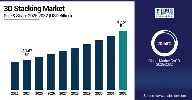
The 3D Stacking Market size was valued at USD 1.67 Billion in 2024 and is projected to reach USD 7.51 Billion by 2032, growing at a CAGR of 20.68% during 2025-2032. The 3D Stacking market is experiencing robust growth driven by rising demand for compact, high-performance, and energy-efficient semiconductor solutions. As traditional 2D scaling faces physical limits, 3D stacking technologies such as through-silicon vias (TSVs), hybrid bonding, and advanced chiplet integration are enabling greater functional density and bandwidth within smaller footprints. These innovations are particularly critical in high-performance computing, AI accelerators, and mobile SoCs, where performance-per-watt is essential.
To Get more information on 3D-Stacking-Market- Request Free Sample Report
The shift toward vertically integrated architectures also improves signal integrity and reduces latency, making them ideal for memory-logic integration and heterogeneous computing. Foundries and IDMs are heavily investing in R&D and production capabilities to support complex multi-die packages, positioning 3D stacking as a foundational element in next-generation semiconductor design and manufacturing.
In 2024, AMD's Ryzen 9000X3D will truely flip the 3D V-Cache hierarchy and have the L3 cache beneath the CCDs allowing for better thermals and a better boost clock speed. This architectural transition solves heat dissipation problems that plagued previous X3D chips and represents a true first in 3D stacking and packaging.
The U.S 3D Stacking market size was valued at USD 0.30 Billion in 2024 and is projected to reach USD 1.41Billion by 2032, growing at a CAGR of 21.39% during 2025-2032. 3D Stacking Market growth is mainly driven by the growing demand for high-performance and energy-efficient semiconductor devices globally across AI, data center and edge computer applications. A full 3D stacking of complex heterogeneous chip structures is fast becoming an ideal choice, to escape from the constraints of traditional 2D scaling, thus pushing the adoption of TSVs, hybrid bonding and advanced interposers as a natural choice for 3D stacking technologies. Additionally, strong investments in U.S. seamless integration of 3D stacked solutions in consumer and enterprise-grade devices powered by an uptick in semiconductor R&D, government incentives for localized chip-manufacturing and a pressing imperative for low-latency and high bandwidth.
The 3D Stacking market trends include the rising adoption of increasing chiplet architecture-based adoption, hybrid bonding offsetting TSV-based bonding methodologies, and further stacking of logic and memory die for performance enhancements and efficiencies. Thermal management and interconnect density innovations will be driven by greater AI, HPC, and 5G requirements Several foundries have also adopted emerging heterogeneous packaging solutions to enable smaller, power-efficient systems.
3D Stacking Market Dynamics:
Drivers:
-
Rising Demand for High Efficiency Drives Adoption of Ultra-Thin Layer 3D Stacking
The growth of 3D stacking is powered by the development of processes for ultra-thin transistor layer transfer for finer 3D vertical integration of components. Due to the intensifying trend of device miniaturization, and the simultaneous increasing demand for higher performance and lower power consumption, fault-tolerant and gate-compatible 3D IC technology may be the only viable alternative to traditional 2D scaling, which has physical limits. Ultra-thin substrate engineering responds with 5nm to 1µm thick transfers of transistor layers on many different types of wafers, with extreme precision and minimum stress. This move enables more system-level integration enabling 3D architectures e.g. vertical FETs with backside power delivery networks. It is a reaction to the demand for higher performance with lower power in a smaller area, so it leads to a new family of heterogeneous semiconductor systems tuned for AI, edge, mobile, and automotive applications.
Restraints:
-
Thermal and Structural Complexities Limit Widespread 3D Stacking Integration
As chip architectures evolve toward denser vertical integration, challenges in heat dissipation and structural alignment become more pronounced. The need for precise bonding of ultra-thin layers introduces design complexities that demand advanced materials, equipment, and process control. These intricate requirements result in higher production costs, longer development cycles, and potential yield issues. Consequently, market scalability is affected, especially in applications where reliability, cost-efficiency, and thermal stability are critical. These limitations slow down the transition from conventional 2D architectures to fully optimized 3D stacked systems across diverse high-performance computing and mobile platforms.
Opportunities:
-
Rising AI Workload Complexity Drives Demand for Advanced 3D Stacking Architectures
by the growing demand of advanced AI and high-performance computing workloads, creating an urgent necessity for 3D stacking solutions. The use case for this demand shift is further driven by the requirements to alleviate bottlenecks from transmitting data, increase bandwidths, and above beneficial aspects of energy efficiency needed in dense systems. With 3D Stacking, GPU core, memory, and photonics can be integrated vertically, supporting high-density compact designs with enhanced performance. For AI accelerators in edge devices and data centers with tight latency and power requirements, these capabilities unlock a range of new possibilities. To meet the demand for rapid, scalable computing from emerging industries, 3D stacking emerges as one of the primary drivers of next generation semiconductor performance and a catalyst for significant innovation and investment at all levels of the global electronics ecosystem.
Some of the high-speed interconnects that Nvidia is developing for its next-gen 3D-stacked AI accelerators will be based in integrated silicon photonics to improve performance and energy efficiency. They developed an architecture that stacks GPUs, DRAM, and optical interfaces to leverage efficient high-bandwidth and low-latency AI compute systems.
Challenges:
-
Increased Thermal and Manufacturing Complexity Slows 3D Stacking Market Expansion
While 3D stacking offers enhanced performance and miniaturization benefits, it brings about significant challenges that hinder widespread adoption. As more layers of chips are vertically integrated, effective heat dissipation becomes increasingly difficult, leading to potential performance throttling and reduced reliability. Simultaneously, achieving high manufacturing yields becomes more complex due to intricate layer alignment and greater sensitivity to defects. These technical challenges result in higher production costs and the need for advanced cooling and fabrication technologies. As a result, scalability becomes limited, especially for mainstream and cost-sensitive applications. Unless these thermal and yield-related issues are mitigated, they will continue to restrict the growth trajectory of the 3D stacking market.
3D Stacking Market Segmentation Analysis:
By Method
In 2024, the Die-to-Die segment accounted for approximately 24% of the 3D Stacking Market share, supported due to increasing high-performance computing (HPC) demands owing to AI, data center and 5G application growths. As a point of modularity and scalability for next-generation chip designs, it is able to provide low-latency, high-bandwidth interconnects between heterogeneous dies.
The Wafer-to-Wafer segment is expected to experience the fastest growth in 3D Stacking Market over 2025-2032 with a CAGR of 23.92%, owing to vertical integration, lower form factor and better performance. The rising demand is propelled by higher adoption in high-density memory and logic devices as well as image sensors — especially for Artificial Intelligence (AI), Internet of Things (IoT), and mobile applications. This method is also compatible with high yield and low-cost, which are attractive for volume-production.
By Interconnecting Technology
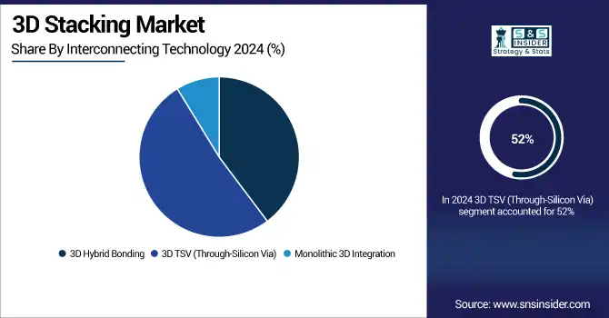
In 2024, the 3D TSV (Through-Silicon Via) segment accounted for approximately 52% of the 3D Stacking Market share, The increasing demand for high-performance computing, AI accelerators, and advanced memory packaging is promoting adoption. TSV technology provides vertical interconnects, helping to reduce latency and power consumption in tight-constraint chip designs.
The Monolithic 3D Integration segment is expected to experience the fastest growth in 3D Stacking Market over 2025-2032 with a CAGR of 26.92%, due to its ability to enable ultra-dense integration at the transistor level. This approach reduces interconnect delay and power consumption while improving overall device performance. Increasing demand for miniaturized, energy-efficient chips in AI, IoT, and mobile devices is accelerating adoption of monolithic 3D architectures across advanced semiconductor applications.
By Device Type
In 2024, the Logic ICs segment accounted for approximately 36% of the 3D Stacking Market share, owing to increased demand for High-Performance Computing and the fact that AI workloads require significant processing capacity with low latency and faster data processing time. This level of 3D stacking is great for logic chips because it can benefit from high bandwidth and low power consumption which is essential for modern processors and data centre applications. Furthermore, the demand for miniaturized and high-density chip solutions in consumer appliances also increases the growth of this segment.
The MEMS/Sensors segment is expected to experience the fastest growth in 3D Stacking Market over 2025-2032 with a CAGR of 23.20%, due to growing need for novel, compact and multifunctional sensors in smartphones, automotive electronics and IoT devices. Due to the 3D stacking MEMS gain in more chips performance and compact size as sensing elements and signal processing circuitry can be integrated on substrate with a smaller footprint. The move towards more smart, connected systems, and autonomous technologies is accelerating the consumerization of advanced sensor solutions that gain from 3D integration for improved efficiency, reliability, and responsiveness.
By End Use
In 2024, the Consumer Electronics segment accounted for approximately 32% of the 3D Stacking Market share, due to increased consumer demand mainly towards energy-efficient devices such as smartphones, wearables as well as tablets, while also incorporating high-performance computing into these compact devices. Q: What is 3D stacking technology and what are its advantages? The use of 3D integrated solutions in electronic product design is being driven by the rising consumer demand for sophisticated capabilities such as AI processing, 4K and above resolution displays, and high-speed data transfer.
The Communications (Telecommunication, Data Centres & HPC) segment is expected to experience the fastest growth in 3D Stacking Market over 2025-2032 with a CAGR of 23.52%, fueled by increasing demand for faster data processing, higher bandwidth, and energy-efficient solutions. The surge in 5G deployment, edge computing, and AI-driven data centers is accelerating the adoption of 3D stacked architectures, which offer enhanced performance and lower latency. This segment benefits from innovations in chiplet integration and vertical stacking, which support complex, high-throughput communication tasks in compact footprints.
3D Stacking Market Regional Outlook:
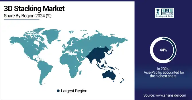
In 2024 Asia-Pacific dominated the 3D Stacking Market and accounted for 44% of revenue share. This dominance is driven by the region’s robust semiconductor manufacturing ecosystem, strong presence of leading foundries, and significant investments in advanced packaging technologies. Countries like Taiwan, South Korea, China, and Japan are at the forefront of chip innovation, supported by government initiatives, rising demand for AI and 5G infrastructure, and the expansion of consumer electronics production.
North America is expected to witness the fastest growth in the 3D Stacking Market over 2025-2032, with a projected CAGR of 22.56%, owing to growing investment in Ai, high-performance computing, and advanced packaging by Intel, AMD, NVIDIA, and the other key players. The region is fueled by a well-established R&D infrastructure, high demand for chip miniaturization, and government efforts to achieve semiconductor self-sufficiency. Strong uptake of 3D packaging in data center and Defence electronics further fuels the market accelerators.
In 2024, Europe emerged as a promising region in the 3D Stacking Market, driven by increased investments in semiconductor R&D, a growing emphasis on chip sovereignty, and the development of AI and IoT ecosystems. Countries like Germany, France, and the Netherlands are enhancing capabilities in advanced packaging, supported by EU initiatives such as the European Chips Act. The region is witnessing rising demand from automotive electronics, industrial automation, and medical device sectors, positioning Europe as a key growth contributor in the global 3D stacking landscape.
LATAM and MEA are experiencing steady growth in the 3D Stacking Market, owing to the rising adoption of advanced electronics, telecom infrastructure, and increasing demand for consumer devices. By March 2023, North America and in particular the United States began to significantly increase government and private sector initiatives to boost digital transformation that will improve the semiconductor ecosystem via more investments in their data centers and smart technologies in line with other regions. Although the markets are relatively immature and at an early stage of developing demand for these compact, high-performance computing solutions, 3D stacking technologies represent a long-term opportunity in these emerging markets.
Get Customized Report as per Your Business Requirement - Enquiry Now
3D Stacking Companies are:
The 3D Stacking Market Companies are Samsung Electronics, TSMC, Micron Technology, SK Hynix, AMD, NVIDIA, Sony Semiconductor Solutions, IBM, Broadcom, Kioxia, Western Digital, OmniVision Technologies, ASE Technology Holding, Amkor Technology, Xperi, JCET Group, SPIL, Entegris, Marvell Technology, Intel Corporation and Others.
Recent Developments:
-
In June 2025, Sony Semiconductor Solutions has unveiled the IMX479 stacked SPAD sensor, boosting automotive LiDAR with faster, high-resolution depth detection. Its advanced Cu-Cu interconnects and compact design enhance ADAS and autonomous driving capabilities with improved range and precision.
-
In April 2025, SK Hynix plans to revolutionize AI memory with vertically stacked 3D HBM5, aiming for reduced latency and higher efficiency. This strategic move targets dominance in next-gen AI chips amid intensifying 3D packaging competition.
| Report Attributes | Details |
|---|---|
| Market Size in 2024 | USD 1.67 Billion |
| Market Size by 2032 | USD 7.51 Billion |
| CAGR | CAGR of 20.68% From 2025 to 2032 |
| Base Year | 2024 |
| Forecast Period | 2025-2032 |
| Historical Data | 2021-2023 |
| Report Scope & Coverage | Market Size, Segments Analysis, Competitive Landscape, Regional Analysis, DROC & SWOT Analysis, Forecast Outlook |
| Key Segments | • By Method (Die-to-Die, Die-to-Wafer, Wafer-to-Wafer, Chip-to-Chip and Chip-to-Wafer) • By Interconnecting Technology(3D Hybrid Bonding, 3D TSV (Through-Silicon Via) and Monolithic 3D Integration) • By Device Type(Logic ICs, Imaging & Optoelectronics, Memory Devices, MEMS/Sensors, LED and Others (RF, photonics, analog & mixed signals, and power devices)) • By End Use(Consumer Electronics, Manufacturing, Communications (Telecommunication, Data Centres & HPC), Automotive, Medical Devices/Healthcare and Others (Military & Defence, Aviation)) |
| Regional Analysis/Coverage | North America (US, Canada), Europe (Germany, UK, France, Italy, Spain, Russia, Poland, Rest of Europe), Asia Pacific (China, India, Japan, South Korea, Australia, ASEAN Countries, Rest of Asia Pacific), Middle East & Africa (UAE, Saudi Arabia, Qatar, South Africa, Rest of Middle East & Africa), Latin America (Brazil, Argentina, Mexico, Colombia, Rest of Latin America). |
| Company Profiles | The 3D Stacking Market Companies are Samsung Electronics, TSMC, Micron Technology, SK Hynix, AMD, NVIDIA, Sony Semiconductor Solutions, IBM, Broadcom, Kioxia, Western Digital, OmniVision Technologies, ASE Technology Holding, Amkor Technology, Xperi, JCET Group, SPIL, Entegris, Marvell Technology, Intel Corporation and Others. |
Frequently Asked Questions
Ans: Asia- Pacific dominated the 3D Stacking Market in 2024.
Ans: The “3D TSV (Through-Silicon Via)” segment dominated the 3D Stacking Market
Ans: Rising demand for high-performance, compact, and energy-efficient semiconductor devices is the key driver of the 3D Stacking Market.
Ans: The 3D Stacking Market size was valued at USD 1.67 Billion in 2024 and is projected to reach USD 7.51 Billion by 2032
Ans: The 3D Stacking Market is expected to grow at a CAGR of 20.68% during 2025-2032.
Get in Touch
