
Advanced Packaging Market Report Scope & Overview:
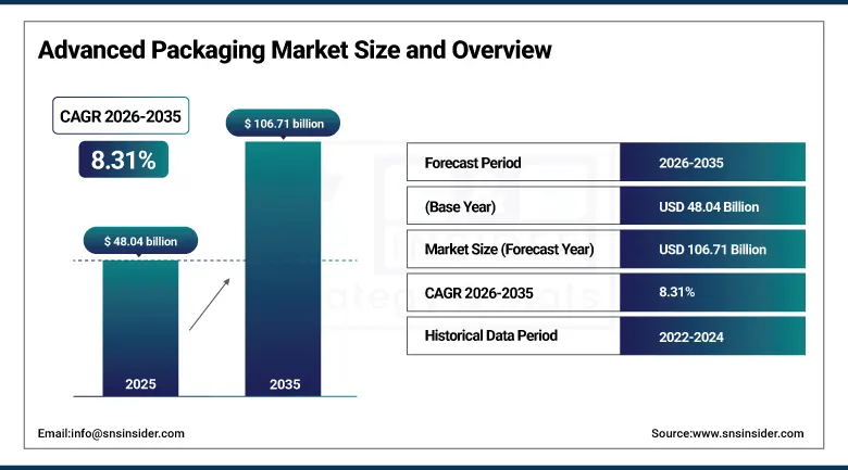
The Advanced Packaging Market size was valued at USD 48.04 Billion in 2025 and is expected to reach USD 106.71 Billion by 2035, growing at a CAGR of 8.31% from 2026–2035.
The global advanced packaging market is growing at a sustained and commercially significant pace. Advanced packaging refers to semiconductor packaging technologies beyond conventional wire-bond and lead-frame approaches, encompassing flip-chip interconnects, fan-out and fan-in wafer-level packaging, 2.5D interposer-based multi-chip modules, 3D through-silicon-via stacked dies, system-in-package heterogeneous integration, and emerging hybrid bonding architectures whose sub-micron interconnect pitch enables AI accelerator performance levels that monolithic scaling can no longer economically deliver.
In 2024, TSMC expanded its CoWoS (Chip-on-Wafer-on-Substrate) advanced packaging capacity by approximately 60% to address surging AI accelerator demand from NVIDIA, AMD, and major cloud hyperscalers whose H100, MI300, and custom AI chip programmes require CoWoS 2.5D interposer packaging for HBM memory integration. The capacity expansion reflects the commercial urgency created by the AI infrastructure investment cycle whose advanced packaging bottleneck became a critical supply constraint limiting AI accelerator production ramp during peak demand from cloud providers’ AI buildout.
Market Size and Forecast
-
Market Size in 2026E: USD 52.03 Billion
-
Market Size by 2035: USD 106.71 Billion
-
CAGR: 8.31% from 2026 to 2035
-
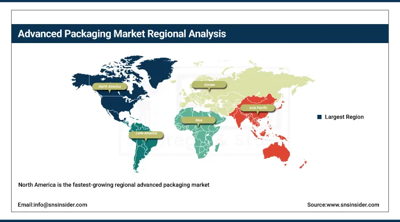
Fastest Growing Region: North America
-
Largest Region: Asia Pacific
To Get more information on Advanced Packaging Market - Request Free Sample Report
Advanced Packaging Market Trends
-
Growing adoption of heterogeneous chiplet architectures is driving demand for advanced packaging technologies that enable high-performance multi-die integration and improved manufacturing efficiency
-
Integration of High Bandwidth Memory (HBM) with AI accelerators is creating strong demand for advanced 2.5D and 3D packaging solutions in high-performance computing applications
-
Fan-out panel-level packaging (FO-PLP) is gaining traction as a cost-effective packaging approach that improves scalability and reduces manufacturing costs
-
Increasing deployment of silicon carbide power modules in electric vehicles and charging infrastructure is accelerating demand for advanced packaging technologies with superior thermal and reliability performance
-
Hybrid bonding technology is emerging as a next-generation packaging solution that enables ultra-high-density interconnects and advanced 3D integrated circuit architectures
U.S. Advanced Packaging Market Size Outlook:
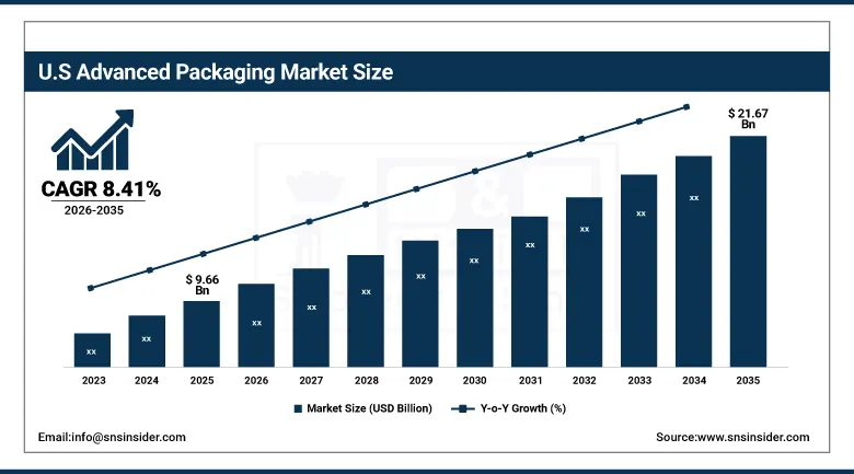
The U.S. Advanced Packaging Market is estimated to be USD 9.66 Billion in 2025 and is projected to reach USD 21.67 Billion by 2035, growing at a CAGR of 8.41% during 2026–2035.
The U.S. Advanced Packaging Market is the most commercially significant national market within the fastest-growing North American region. Intel Foundry Services’ EMIB and Foveros packaging technologies, NVIDIA’s CoWoS procurement from TSMC and ASE, AMD’s 3D V-Cache packaging, and Apple’s SiP-integrated Apple Silicon collectively define the U.S. advanced packaging commercial landscape. The CHIPS and Science Act’s USD 52 billion investment including domestic advanced packaging investment incentive creates structured government-supported demand that sustains commercial relationships with OSAT capacity expansion in the United States.
Intel announced production deployment of its Foveros Direct 3D advanced packaging technology in 2024, enabling direct copper-to-copper hybrid bonding at sub-10-micron pitch for its Meteor Lake and Lunar Lake client processor dies. The hybrid bonding’s elimination of microbumps creates die-to-die interconnect density 1000x above conventional flip-chip alternatives, enabling compute die and SoC die integration at a pitch previously only achievable within a single monolithic die and creating commercial differentiation that sustains Intel Foundry’s advanced packaging service positioning.
Advanced Packaging Market Segment Analysis
-
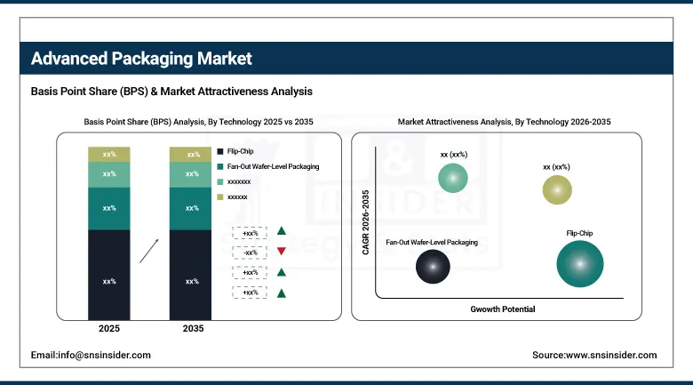
By Technology, the Flip-Chip segment dominated the Advanced Packaging Market with approximately 38% share in 2025, while the Fan-Out Wafer-Level Packaging (FOWLP) segment is the fastest growing.
-
By End-User Industry, the Consumer Electronics segment dominated the Advanced Packaging Market with 48.77% share in 2025, while the Automotive & EV segment is the fastest growing.
-
By Application, the Smartphones & Consumer Electronics segment dominated the Advanced Packaging Market with approximately 45%, while the High-Performance Computing & AI Accelerators segment is the fastest growing.
-
By Integration Level, the 2D IC segment dominated the Advanced Packaging Market with approximately 62% share in 2025, while the 3D IC segment is the fastest growing.
By Technology, flip-chip dominates, FOWLP grows fastest
Flip-chip retained the dominant technology position with approximately 38% of the advanced packaging market in 2025. Flip-chip’s commercial primacy reflects its role as the most commercially mature and widely deployed advanced packaging technology whose 30-year production history creates supply chain depth, equipment availability, and process knowledge that newer alternatives cannot match at equivalent commercial scale. Each advanced microprocessor, GPU, and RF IC that specifies controlled-collapse chip connection (C4) or copper pillar bump flip-chip interconnect creates procurement whose aggregate across the global semiconductor industry’s high-performance IC production creates commercial scale. NVIDIA’s GPU, Intel’s processor, Qualcomm’s mobile AP, and Broadcom’s networking IC programmes collectively represent flip-chip’s dominant application portfolio whose commercial scale defines the technology’s market leadership.
Fan-out wafer-level packaging is the fastest-growing technology because 5G modem integration, AI edge inference chip’s compact form factor requirement, and the wearable’s ultra-thin SiP integration create application-driven specification motivation for FOWLP’s die redistribution without substrate approach. TSMC’s InFO, Samsung’s FoCoS, and ASE’s FOCoS technologies demonstrate the commercial ecosystem whose capability creates specification accessibility for diverse IC types beyond the smartphone AP’s initial FOWLP adoption.
By End User, consumer electronics dominates, automotive grows fastest
Consumer electronics retained the dominant end-user position with 48.77% of the advanced packaging market in 2025. The smartphone’s advanced AP, modem, RF front-end module, PMIC, and memory packaging creates per-device advanced packaging procurement whose aggregate across approximately 1.2 billion annual smartphone shipments creates the most commercially significant end-user procurement category. Tablet, laptop, and wearable device’s growing semiconductor integration creates secondary consumer electronics procurement that compounds with smartphone volume. Apple’s SiP-integrated Apple Watch, the M-series MacBook’s monolithic die packaging, and iPhone’s CoWoS AP collectively demonstrate the commercial breadth of consumer electronics’ advanced packaging portfolio.
Automotive and EV is the fastest-growing end user because silicon carbide power module’s copper-pillar and silver-sintering interconnect requirement, ADAS processor’s thermal management demand, and the EV’s extraordinary per-vehicle semiconductor content increase from approximately USD 500 in ICE vehicles to USD 1,200+ in EVs create above-average automotive advanced packaging procurement. Each new EV model that specifies advanced SiC inverter packaging creates procurement whose per-vehicle advanced packaging content compounds with EV adoption’s extraordinary commercial pace.
By Application, smartphones dominate, AI accelerators grow fastest
Smartphones and consumer electronics retained the dominant application position with approximately 45% of the advanced packaging market in 2025. The smartphone application’s per-device advanced packaging complexity, whose AP-SoC flip-chip, FOWLP modem, RDL-integrated RF front-end, and stacked LPDDR packaging create multi-technology procurement per handset, creates commercial density that high-performance computing’s lower unit volume cannot match by aggregate commercial contribution. Each new smartphone generation’s die count increase and performance advancement creates advanced packaging specification upgrade whose commercial value compounds with the annual smartphone replacement cycle.
High-performance computing and AI accelerators are the fastest-growing application because the AI infrastructure investment cycle’s extraordinary commercial momentum creates the most commercially premium per-package advanced packaging demand in the market’s history. Each NVIDIA H100/H200 and B100/B200 GPU that requires CoWoS 2.5D packaging for HBM integration creates per-package advanced packaging procurement whose commercial value at thousands of dollars per packaged unit substantially exceeds smartphone AP packaging alternatives. The hyperscaler’s AI cluster investment, whose per-rack advanced packaging content compounds with cluster scale, creates commercial demand that sustains TSMC’s, ASE’s, and Amkor’s extraordinary advanced packaging capital investment.
By Integration, 2D IC dominates, 3D IC grows fastest
Two-dimensional IC packaging retained the dominant integration position with approximately 62% of the advanced packaging market in 2025. 2D IC’s commercial primacy reflects the established flip-chip, wafer-level, and single-die packaging supply chain whose commercial maturity creates procurement accessibility for the entire semiconductor industry beyond the most advanced packaging applications. Each commodity microcontroller, power management IC, and standard logic device that specifies 2D advanced packaging creates procurement volume whose aggregate across the global semiconductor industry’s diverse IC portfolio creates commercial scale that 3D IC’s higher-value but lower-volume applications cannot match.
3D IC is the fastest-growing integration level because AI accelerator’s HBM memory stack, AMD’s 3D V-Cache processor, and Sony’s image sensor backside illumination stacking create diverse commercial applications whose premium per-unit commercial value sustains the 3D IC’s above-average market growth. Each new AI training chip that integrates HBM3E through CoWoS or SoIC creates 3D IC packaging procurement whose commercial scale compounds with AI infrastructure’s extraordinary investment pace.
Regional Insights
|
Region |
Major Country |
Share within Region, 2025 (%) |
|---|---|---|
|
North America |
United States |
87.4% |
|
Europe |
Germany |
22.3% |
|
Asia Pacific |
Taiwan |
38.4% |
|
Middle East & Africa |
Israel |
31.2% |
|
Latin America |
Brazil |
44.2% |
North America Advanced Packaging Market Insights
North America is the fastest-growing regional advanced packaging market, driven by CHIPS Act domestic advanced packaging investment, Intel’s Foveros and EMIB technology deployment, and the AI accelerator demand’s supply chain localisation motivation. The United States accounts for approximately 87.4% of North American revenues through Intel Foundry Services, Amkor’s Tempe Arizona facility, and the AI semiconductor programme’s TSMC Arizona advanced packaging investment.
Canada contributes approximately 12.6% of North American revenues through its semiconductor design community’s packaging procurement and the growing advanced electronics manufacturing investment.
Get Customized Report as per Your Business Requirement - Enquiry Now
Europe Advanced Packaging Market Insights
Europe is a technically sophisticated advanced packaging market where Infineon’s power semiconductor packaging, IMEC’s advanced packaging research, and ASE’s European operations create structured institutional demand. Germany accounts for approximately 22.3% of European revenues through Infineon’s SiC power module advanced packaging, Bosch’s automotive semiconductor packaging, and the automotive sector’s premium advanced packaging specification.
The Netherlands, France, and Ireland are significant secondary markets where NXP Semiconductors, STMicroelectronics, and Intel’s Leixlip facility create consistent advanced packaging procurement.
Asia Pacific Advanced Packaging Market Insights
Asia Pacific dominated the global advanced packaging market in 2025 with the highest revenue share, reflecting the concentration of the world’s leading OSAT companies, semiconductor foundries, and consumer electronics manufacturing. Taiwan accounts for approximately 38.4% of Asia Pacific revenues through TSMC’s CoWoS, InFO, and SoIC advanced packaging leadership, ASE Group’s comprehensive OSAT service portfolio, and SPIL’s packaging operations whose combined service revenue creates Asia Pacific’s commercial dominance.
South Korea’s Samsung Electro-Mechanics and SK Hynix’s HBM packaging, China’s growing domestic OSAT ecosystem, and Japan’s Amkor and Renesas advanced packaging create significant secondary markets whose combined procurement sustains Asia Pacific’s dominant regional position.
MEA & Latin America Advanced Packaging Market Insights
Israel leads MEA revenues at approximately 31.2% through Intel’s Kiryat Gat facility, Tower Semiconductor’s advanced packaging service, and the semiconductor design community’s packaging procurement. Brazil leads Latin American revenues at approximately 44.2% through its electronics manufacturing sector’s semiconductor assembly and the consumer electronics distribution market’s advanced IC procurement.
Market Dynamics
Growth Drivers: AI accelerator heterogeneous integration demand and 5G device miniaturisation requiring advanced packaging
Increasing demand for miniaturisation and performance improvements in electronic devices is the advanced packaging market’s most commercially certain structural growth driver. The AI infrastructure investment cycle’s extraordinary scale, whose hyperscaler procurement of AI accelerators requiring CoWoS 2.5D packaging with HBM creates the most commercially premium advanced packaging demand, sustains TSMC’s, ASE’s, and Amkor’s extraordinary capacity investment. Each new AI data centre deployment creates advanced packaging procurement whose per-rack semiconductor content compounds with the extraordinary global AI infrastructure buildout.
5G adoption’s semiconductor integration requirement, whose modem and RF front-end module’s heterogeneous integration demands fan-out wafer-level packaging’s compact die embedding, creates consumer electronics advanced packaging demand that compounds with each new 5G smartphone generation. The surge in 5G subscriptions from 12 million toward 4.5 billion creates proportional advanced packaging demand whose commercial momentum sustains market growth.
Restraints: High capital expenditure for advanced packaging capacity and supply chain concentration in Asia Pacific
Advanced packaging capacity investment’s extraordinary capital intensity, whose CoWoS line installation requires USD 1-3 billion per manufacturing facility, creates supply constraint risk whose lead time from investment decision to production capacity creates supply-demand imbalance during rapid AI infrastructure demand acceleration. Each advanced packaging supply bottleneck that constrains AI accelerator production creates commercial urgency that sustains premium pricing but moderates the volume growth that additional capacity would enable.
Asia Pacific’s concentration of over 80% of global OSAT capacity creates supply chain geopolitical risk whose Taiwan and South Korea concentration creates sovereign risk motivation for domestic advanced packaging capacity investment in North America and Europe whose build-out investment creates transitional supply constraint.
Opportunities: Domestic advanced packaging investment under CHIPS Act and SiC automotive power module premium market
CHIPS and Science Act’s USD 52 billion domestic semiconductor investment, whose advanced packaging component creates structured U.S. OSAT capacity development, represents the most commercially certain near-term market development whose government-supported investment creates new North American supply capacity. Each new domestic advanced packaging facility commissioned creates commercial procurement relationships whose U.S. government customers’ security clearance requirements create captive demand.
Silicon carbide power module advanced packaging for EV inverter represents the most commercially premium automotive opportunity whose copper-pillar, silver-sintering, and direct-bond-copper interconnect specifications create per-module packaging commercial value substantially above conventional silicon power device packaging alternatives.
Recent Developments:
-
2024: TSMC expanded its CoWoS advanced packaging capacity by approximately 60% in 2024 to address surging AI accelerator demand from NVIDIA, AMD, and hyperscaler custom chip programmes requiring 2.5D interposer packaging for HBM memory integration.
-
2024: Intel announced production deployment of Foveros Direct 3D advanced packaging technology in 2024 enabling direct copper-to-copper hybrid bonding at sub-10-micron pitch for Meteor Lake and Lunar Lake client processor heterogeneous chiplet integration.
-
2024: ASE Group expanded its fan-out panel-level packaging capacity in 2024 with new FOPLP production lines targeting cost-sensitive advanced packaging applications in IoT, wearable, and mid-range smartphone markets whose panel-substrate economics create lower per-die packaging cost.
Advanced Packaging Companies are:
-
Taiwan Semiconductor Manufacturing Company (TSMC)
-
Amkor Technology Inc.
-
Intel Corporation (Intel Foundry Services)
-
Samsung Electronics Co., Ltd.
-
SPIL (Siliconware Precision Industries Co., Ltd.)
-
Powertech Technology Inc. (PTI)
-
JCET Group Co., Ltd.
-
Longcheer Technology
-
Tongfu Microelectronics (TFME)
-
Hua Tian Technology Co., Ltd.
-
Unisem Group
-
UTAC Holdings Ltd.
-
Lingsen Precision Industries Ltd.
-
ChipMOS Technologies Inc.
-
KYEC (King Yuan Electronics Co., Ltd.)
-
Nepes Corporation
-
Shinko Electric Industries Co., Ltd.
-
Ibiden Co., Ltd.
Advanced Packaging Market Report Scope
| Report Attributes | Details |
|---|---|
| Market Size in 2025 | USD 48.04 Billion |
| Market Size by 2035 | USD 106.71 Billion |
| CAGR | CAGR of 8.31% From 2026 to 2035 |
| Base Year | 2025 |
| Forecast Period | 2026-2035 |
| Historical Data | 2022-2024 |
| Report Scope & Coverage | Market Size, Segments Analysis, Competitive Landscape, Regional Analysis, DROC & SWOT Analysis, Forecast Outlook |
| Key Segments | • by Technology (Flip-Chip, Fan-Out Wafer-Level Packaging/FOWLP, Fan-In Wafer-Level Packaging/FIWLP, 2.5D/3D IC, Embedded Die, System-in-Package/SiP, Chip-on-Wafer-on-Substrate/CoWoS, Others) • by Application (Smartphones & Consumer Electronics, Automotive/EV Power Modules, High-Performance Computing/AI Accelerators, Data Centre & Cloud Infrastructure, 5G & Telecommunications, Healthcare & Medical Devices, Aerospace & Defence, Others) • by End-User Industry (Consumer Electronics, Automotive & EV, IT & Computing/Data Centres, Telecommunications, Healthcare, Aerospace & Defence, Others) |
| Regional Analysis/Coverage | North America (US, Canada, Mexico), Europe (Eastern Europe [Poland, Romania, Hungary, Turkey, Rest of Eastern Europe] Western Europe] Germany, France, UK, Italy, Spain, Netherlands, Switzerland, Austria, Rest of Western Europe]), Asia Pacific (China, India, Japan, South Korea, Vietnam, Singapore, Australia, Rest of Asia Pacific), Middle East & Africa (Middle East [UAE, Egypt, Saudi Arabia, Qatar, Rest of Middle East], Africa [Nigeria, South Africa, Rest of Africa], Latin America (Brazil, Argentina, Colombia, Rest of Latin America) |
| Company Profiles | Taiwan Semiconductor Manufacturing Company (TSMC), ASE Technology Holding Co., Ltd., Amkor Technology Inc., Intel Corporation (Intel Foundry Services), Samsung Electronics Co., Ltd., SK Hynix Inc., SPIL (Siliconware Precision Industries Co., Ltd.), Powertech Technology Inc. (PTI), JCET Group Co., Ltd., Longcheer Technology, Tongfu Microelectronics (TFME), Hua Tian Technology Co., Ltd., Unisem Group, UTAC Holdings Ltd., Lingsen Precision Industries Ltd., ChipMOS Technologies Inc., KYEC (King Yuan Electronics Co., Ltd.), Nepes Corporation, Shinko Electric Industries Co., Ltd., Ibiden Co., Ltd. |

Frequently Asked Questions
The Advanced Packaging Market is expected to grow at a CAGR of 8.31% from 2026 to 2035.
The Advanced Packaging Market was valued at USD 48.04 Billion in 2025.
Increasing demand for miniaturisation and performance improvements in electronic devices and heterogeneous chiplet integration for AI accelerators, and embedded die packaging for 5G compactness requirements.
Consumer Electronics dominated the Advanced Packaging Market with 48.77% share in 2025 as confirmed by SNS Insider, while Automotive & EV is the fastest growing end-user segment.
Asia Pacific dominated the Advanced Packaging Market in 2025 with the highest revenue share, while North America is the fastest-growing region driven by CHIPS Act domestic advanced packaging investment and AI accelerator demand.
