Atomic Force Microscopy Market Report Scope & Overview:
Get more information on Atomic Force Microscopy Market - Request Sample Report
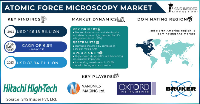
The Atomic Force Microscopy Market size is expected to be valued at USD 82.94 Billion in 2023. It is estimated to reach USD 146.18 Billion by 2032 with a growing CAGR of 6.5% over the forecast period 2024-2032.
The AFM market is on the rise as technology sees increased use in its openings in multiple industries ranging from semiconductors, to life sciences, materials science, and nanotechnology. The growth is primarily driven by the developing need for imaging and surface analysis at the nanoscale. AFM is the primary factor that advances nanotechnology research, especially in the semiconductor manufacturing and life sciences markets. The market boosts are primarily due to the usefulness of AFM in the growing practice of micro-electromechanical systems and microelectronics in the life sciences and quality assurance and failure analysis in the semiconductor sector. Further, the current advancements in the technology, such as the rapid high-speed AFM development expand on its capabilities and its areas of application. A great example of the marvels modern technology SSD is the creation of a new type of AFM, the high-resolution imaging Forster resonant energy high-speed massively parallel H+AFM or HS-AFM. A group of researchers from the National Taiwan University and other organizations recently developed a cheap, publicly available high-speed AFM known as the HS-AFM. This breakthrough technology costs less than USD 4,000 and obtains high-resolution images better than traditional AFMs, which can cost from USD 100,000 and above. The HS-AFM is able to produce an accurate nanoscale image relatively quickly while using a small amount of the costly cantilever tips. A great example of the technology’s use is the assessment of the severity of atopic dermatitis. The reliance on such cost-effective technologies will see the increased adoption of AFM technologies across various sectors, and the plummeting costs of equipment will see growth in new and existing markets.
The Atomic Force Microscopy market is heading for serious expansion. This is driven by the increasing global focus on nanotechnology research and the complex multidisciplinary approaches adopted by the world’s relevant governments. Like the Canadian government prioritizes making high-resolution microscopy an essential part of and instrument toward achievement of new scientific understanding through interdisciplinary collaboration and investment into cutting-edge technological development, other world governments toe a similar path. In the case of Canada, the government realizes the versatility of nanotechnology in biomedicine, environmental science, and materials engineering and makes a significant effort to help develop the field. In particular, the annual Canadian investment in nanotechnology constitutes USD 45-50 Million, and this is indicative of a general worldwide effort to give proper attention to any kind of research that heavily depends on accurate, reliable imaging provided by cameras or microscopy. The United States’ National Nanotechnology Initiative is another relevant example, being a collaborative initiative of 19 US government agencies to advance nanotechnology and ensure it helps to protect and improve people’s lives while promoting the sustainable health of the environment. The initiative is aimed to provide support for all branches of nano-related research, both basic and applied, and has played a significant role in ensuring the establishment of excellence centers focused on better understanding of nanoscale phenomena. The very structure and focus of government nanotechnology programs, such as Canada’s or United States’, provide significant opportunities for the Atomic Force Microscopy market to grow. For example, the integration of Atomic Force Microscopy techniques into multidisciplinary research has long been the standard and is known to be enabling scientists to see molecules, such as DNA and proteins, like never before. This highly detailed understanding leads to innovations in genomics, pharmaceuticals, and environmental cleanup. It also provides the unprecedented level of structural and mechanical detail of atomic and subatomic structure of new nanomaterial necessary for devising effective risk assessment methodologies for their handling. Thus, as world governments keep investing in nanotechnology one can anticipate that the Atomic Force Microscopy market will grow providing an appreciable fillip to the growth of the market.
Market Dynamics
Drivers
- Progressing the development of diagnosis and treatment with AFMs
In the field of biomedicine, Atomic Force Microscopy (AFMs) are changing the way we can investigate biological samples with exceptional accuracy. AFMs allow researchers to visualize proteins, DNA, and cell surfaces with high precision on a nanometer scale, offering a deeper understanding of intricate biological processes and interactions. This ability is essential for progressing our comprehension of cellular processes, molecular connections, and disease routes. AFMs aid in understanding the relationship between structure and function of biomolecules by visualizing and measuring molecular forces, crucial for creating specific diagnostic tools and therapeutic approaches. The NIH plays a key role in funding AFM research with grants, emphasizing the technology's importance in biomedical progress. One example is how the NIH devotes significant funding to initiatives that utilize AFMs for researching disease mechanisms and creating new treatments. Recent developments involve utilizing AFMs to identify early cancer biomarkers and analyze the mechanical characteristics of cancer cells, crucial for early detection and customized treatment. Moreover, AFMs have a substantial potential to aid in drug development by allowing for the precise monitoring of drug interactions with cell parts, leading to the development of better and more focused medications. The incorporation of AFM technology in biomedicine underlines its crucial impact on shaping the future of diagnostic and therapeutic advancements, aided by ongoing government funding and research initiatives.
- Increasing use in nanotechnology and materials science is propelling growth in the atomic force Microscopy market.
The increased use of atomic force microscopy (AFM) in nanotechnology and materials science is a major factor influencing the AFM market. Nanotechnology, a game-changing industry affecting multiple sectors like healthcare, energy, manufacturing, and consumer goods, heavily depends on AFMs for advancement. This technology plays a crucial role in analyzing materials at the atomic level, which is necessary for creating new materials with specific optical, electrical, and mechanical properties. AFMs provide unmatched clarity in observing objects as tiny as single atoms and collecting precise topographical data on surfaces at the Nano scale. This ability is essential for progress and innovation in areas like carbon nanotubes, nanoparticles, and DNA sequencing, where accurate characterization is critical. Also, AFMs are crucial in nanofabrication processes by regulating feature sizes, etch depths, and uniformity in etching and lithography, guaranteeing the precision and excellence of manufactured nanostructures. The Cypher VRS1250 video-rate AFM from Oxford Instruments Asylum Research is a significant advancement in observing dynamic Nano scale processes, like biochemical reactions and molecular self-assembly, which were previously unattainable. The increasing significance of AFMs in advancing nanotechnology and materials science emphasizes their impact on market expansion. Incorporating AFMs into research and development shows a growing preference for precise analytical methods in nanotechnology and materials science, highlighting their crucial role in the field's progress.
Restraints
- Challenges of high costs and limited accessibility in the Atomic Force Microscope Market
One of the major obstacles in the AFM market is the expensive nature of acquiring and up keeping these advanced tools. AFMs are complex instruments that make use of sophisticated Nano scale technologies to achieve unmatched resolution in imaging and characterization. The intricate nature of these products leads to their high cost, making them unaffordable for numerous small labs and research centers. The high cost of purchasing an AFM system at the start can prevent many organizations and institutions from being able to use these advanced tools. Moreover, the proper functioning and care of AFMs require specialized expertise and well-trained staff, which also adds to the total expenses of using them. The requirement for skilled management and upkeep contributes to the operational costs, making it difficult for smaller organizations to rationalize the expenditure. Furthermore, AFMs have restrictions in specific areas of use, like imaging or analyzing samples in liquid or gaseous conditions. This limitation limits their usefulness in various research situations, additionally restricting their possible market uses.
- Harm caused to samples by Contact-Mode AFM is a limitation in the market.
One major limitation in the atomic force microscope (AFM) industry is the risk of causing damage to samples when employing contact-mode AFM methods. In contact mode, the AFM tip applies a constant and repulsive force on the sample surface, using a feedback loop to maintain either a constant force (constant force mode) or a constant height (constant height mode). Even though this method yields important surface topography information, the continuous contact between the probe and the specimen may result in considerable problems, especially with fragile or soft substances like polymers and biological macro molecules. The friction and adhesion forces present in contact mode can lead to undesired distortion or even damage to the sample, which can affect the precision and trustworthiness of the data collected. This constraint limits the use of contact-mode AFM in specific research situations, especially those dealing with delicate or soft samples. For instance, contact mode is effective for examining solid pharmaceutical formulations and fixed cells, but it is not ideal for imaging live cells or dynamic biological processes that require minimal contact and high precision. Thus, the likelihood of sample damage in contact mode poses a significant hurdle in the widespread adoption of AFMs in various research areas, limiting market expansion.
Segment Analysis
By Type
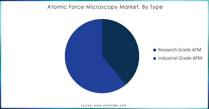
Industrial grade atomic force Microscopy (AFMs) captured the largest revenue share in the atomic force microscopy market, holding 61% of the market in 2023, driven by increasing demand across various manufacturing sectors. These AFMs are tailored for industrial environments, excelling in routine metrology tasks such as surface characterization, thickness measurement, and production process evaluation. The growth of this segment is primarily fueled by the need for precise nano-scale characterization in industries like semiconductor manufacturing, data storage media fabrication, and renewable energy equipment production. Industrial grade AFMs offer high stability, repeatability, and accuracy, essential for quality control and process optimization. They are designed to withstand the rigors of industrial settings, including vibration and temperature fluctuations, and feature user-friendly software interfaces that facilitate operation by non-specialist personnel. Their robust construction ensures durability and reliability in high-volume measurement scenarios. Additionally, advancements such as in-situ imaging capabilities allow for real-time inspection without halting production, further enhancing efficiency and reducing costly reworks. As nanotechnology applications expand, the demand for metrology equipment that can operate effectively in industrial conditions continues to rise. For example, Anton Paar GmbH offers the ToscaTM 400, an advanced AFM designed specifically for industrial applications, providing detailed measurements of nano-surface properties. The growing complexity of nano-scale manufacturing processes underscores the need for precise, high-resolution quality control tools, making industrial grade AFMs pivotal in improving process optimization and ensuring high-quality production standards.
Get Customized Report as per your Business Requirement - Request For Customized Report
By Application
Semiconductor & Electronics is capturing the highest share in Atomic Force Microscope with 37% of share in 2023. AFMs are integral to semiconductor manufacturing, offering non-destructive imaging at atomic or molecular resolutions that is crucial for scaling down device dimensions. This capability is essential for characterizing new materials and understanding surface properties at nanometer scales, which supports the development of high-density, tightly integrated devices. AFMs are extensively used in failure analysis to identify root causes of defects, and they play a vital role in chip fabrication processes such as lithography mask inspection, process monitoring, and quality control. The contactless nature of AFMs allows them to analyze delicate surfaces and temporary structures without causing damage, making them invaluable for next-generation device fabrication. The rapid miniaturization in electronics drives increased AFM usage throughout the fabrication line, from material development to wafer inspection. Key industry players like Bruker Corporation, with its Dimension Icon AFM, and Asylum Research, offering the Cypher VRS, provide advanced AFM solutions tailored for semiconductor applications. These companies’ technologies facilitate precise measurement and characterization needed to address the technical challenges posed by shrinking device dimensions and increasing complexity. The reliance on AFMs by semiconductor foundries and integrated device manufacturers underscores the critical role of these tools in maintaining high-quality standards and reducing defects as technology evolves. The continued advancements in semiconductor technology and the expansion of electronics applications ensure that AFMs remain a driving force in this sector.
REGIONAL ANALYSIS:
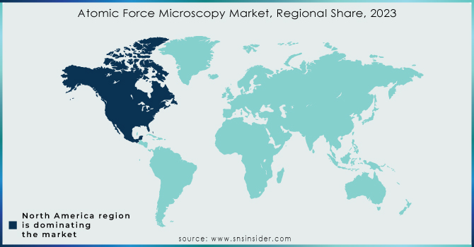
North America dominate the Atomic Force microscope market with 37.20% of share in 2023. This dominance is due to key players such as Bruker Corporation, Park Systems, and WITec, who have established a significant number of AFMs in the area. Strong backing for nanotechnology research from organizations like the National Science Foundation (NSF) has greatly boosted interest in multiple fields, such as life sciences and material science. This funding supports the advancement of high-resolution imaging and analysis for applications like virus detection, material property measurement, and semiconductor analysis, encouraging innovation and development.AFMs are actively utilized for cutting-edge research at universities and national laboratories in the U.S. and Canada, including the National Institutes of Health (NIH) and the National Research Council of Canada (NRC). Examples include the importance of developments in AFM technology, like Bruker’s Dimension Icon and Park Systems' NX10, in the exploration of new fields such as 2D materials and semiconductor device structures. These atomic force Microscopy provide improved features such as high-resolution imaging, advanced force measurements, and real-time data acquisition, facilitating in-depth analysis of nanomaterial and complex semiconductor structures. Advancements in AFM technology, such as the alpha300 R from WITec, have brought about faster imaging and enhanced sensitivity, meeting the demand for accurate analysis in changing research sectors. These innovations guarantee that North America continues to lead in AFM technology, advancing in numerous scientific and industrial uses. North America's strong position in the AFM market is strengthened by the presence of well-established companies, substantial research investments, and constant technological advancements.
Asia Pacific is holding the second largest share for atomic force microscope in 2023. The Asia-Pacific (APAC) region is experiencing substantial growth in the atomic force microscope (AFM) market, driven by massive investments in key industries such as semiconductors, renewable energy, and healthcare. Countries like China, Japan, South Korea, and India are at the forefront of this expansion, with increased demand for nanoscale surface metrology tools like AFMs crucial for material development, quality control, and failure analysis. Active government support for the manufacturing sector, coupled with a high concentration of OEM production units, has significantly augmented this demand. Additionally, the availability of cost-effective AFMs from Chinese manufacturers is making these tools accessible to budget-constrained research organizations and educational institutions, further fueling the market.Regional leaders such as Park Systems (Korea) and Anasys Instruments (US) have capitalized on this growth by establishing local manufacturing and sales facilities. These efforts are not only catering to domestic needs but also supporting the region’s burgeoning export market for AFMs and spare parts. The thriving electronics manufacturing sector in APAC has led to a notable increase in exports, positioning the region as a major player in the global AFM market. Growing collaborations between large firms and academic institutes in APAC are fostering innovative research projects that utilize advanced AFM techniques. This collaborative environment is expected to drive continuous advancements and further strengthen the region's position in the global AFM market. As the demand for high-precision measurement tools expands across various industries, the Asia-Pacific region is poised to become a significant contributor to the growth of the atomic force microscope market in the coming years.
KEY PLAYERS:
The key players in the atomic force microscopy are Bruker, Oxford Instruments, NanoMagnetics Instruments, AFM Workshop, Concept Scientific Instruments, Park Systems, Hitachi High-Tech, Nanonics Imaging, Semilab, Nano Scan Technologies & Other Players.
RECENT DEVELOPMENT
-
In January 2024, Oxford Instruments Asylum Research launched the Cypher ES Battery Edition, a cutting-edge atomic force microscope bundle created specifically for innovative battery research.
-
In June 2021, the Park FX40, a groundbreaking autonomous atomic force microscope (AFM), was introduced by Park Systems in South Korea. The Park FX40 Atomic Force Microscope is notable for being the first AFM to independently carry out all set up and scanning processes.
-
In April 2021, the company Asylum Research, based in the UK, launched the Cypher VRS1250 video-rate atomic force microscope (AFM) manufactured by Oxford Instruments. The new Cypher VRS1250 AFM has twice the speed of its previous model, enabling scan rates of 1250 lines/second and frame rates of 45 frames/second. This increased speed enables scientists to observe tiny details of changing situations that were previously unattainable.
| Report Attributes | Details |
|---|---|
| Market Size in 2023 | USD 82.94 Billion |
| Market Size by 2032 | USD 146.18 Billion |
| CAGR | CAGR of 6.5% From 2024 to 2032 |
| Base Year | 2023 |
| Forecast Period | 2024-2032 |
| Historical Data | 2020-2022 |
| Report Scope & Coverage | Market Size, Segments Analysis, Competitive Landscape, Regional Analysis, DROC & SWOT Analysis, Forecast Outlook |
| Key Segments | • By Type (Research Grade AFM, Industrial Grade AFM) • By Offering (Probes, Atomic Force Microscopes, Software) • By Application (Material Science, Life Sciences, Academics, Semiconductors And Electronics, Others) |
| Regional Analysis/Coverage | North America (US, Canada, Mexico), Europe (Eastern Europe [Poland, Romania, Hungary, Turkey, Rest of Eastern Europe] Western Europe] Germany, France, UK, Italy, Spain, Netherlands, Switzerland, Austria, Rest of Western Europe]), Asia Pacific (China, India, Japan, South Korea, Vietnam, Singapore, Australia, Rest of Asia Pacific), Middle East & Africa (Middle East [UAE, Egypt, Saudi Arabia, Qatar, Rest of Middle East], Africa [Nigeria, South Africa, Rest of Africa], Latin America (Brazil, Argentina, Colombia, Rest of Latin America) |
| Company Profiles | Bruker, Oxford Instruments, NanoMagnetics Instruments, AFM Workshop, Concept Scientific Instruments, Park Systems, Hitachi High-Tech, Nanonics Imaging, Semilab and Nano Scan Technologies. |
| Key Drivers |
|
| Restraints |
|
Frequently Asked Questions
The Atomic Force Microscopy Market size is expected to be valued at USD 82.94 Billion in 2023.
The expected CAGR of the global Atomic Force Microscopy Market during the forecast period is 6.5%.
The Asia Pacific region is anticipated to record the highest Compound Annual Growth Rate (CAGR).
The Atomic Force Microscopes is the leading segment in the market revenue share in 2023.
The North America region with the Highest Revenue share in 2023.
Get in Touch
