
Epitaxial Wafer Market Report Scope & Overview:
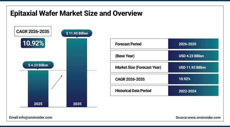
The Epitaxial Wafer Market size was valued at USD 4.23 Billion in 2025 and is expected to reach USD 11.93 Billion by 2035, growing at a CAGR of 10.92% from 2026–2035.
The epitaxial wafers are the customized silicon wafers where a new layer of crystal is added using deposition. Epitaxial wafers give more control to the manufacturer of semiconductors in comparison to regular wafers. That extra layer matters enormously for power semiconductors, LEDs, and MEMS devices, where efficiency, heat conduction, and voltage tolerance directly determine how well the finished chip performs. The demand for the products is rising at an increasing rate along with the automation in industries, electric cars, and consumer electronics, which require semiconductors made using epitaxial wafers that perform better. Furthermore, the development of infrastructure for 5G and IoT is being fueled, but whereas North America is ahead in innovation, the Asia Pacific remains the largest producer of wafers.
Resonac Corporation delivered silicon carbide epitaxial wafers for the inverter driver components in Toyota’s newly released electric car, the Lexus RZ, in March 2023. SiC-enabled inverters increase the fuel efficiency of the car and enhance its range, thereby showing the importance of epitaxial wafers in today’s automobile engineering, with car manufacturers becoming increasingly focused on electrification and squeezing more mileage from battery packs.
To Get More Information On Epitaxial Wafer Market - Request Free Sample Report
Epitaxial Wafer Market Trends
-
Silicon carbide and gallium nitride epitaxial wafers are gaining demand for high-efficiency power electronics, electric vehicles, and industrial applications.
-
Adoption of larger wafer sizes is improving manufacturing efficiency and reducing production costs for high-volume semiconductor fabrication.
-
Expansion of 5G infrastructure is increasing demand for high-quality epitaxial wafers used in RF devices and communication components.
-
Government investments and semiconductor incentive programs are accelerating domestic epitaxial wafer manufacturing capacity across key global markets.
-
Renewable energy and solar power applications are creating new growth opportunities for silicon carbide epitaxial wafers beyond traditional electronics.
U.S. Epitaxial Wafer Market Size Outlook
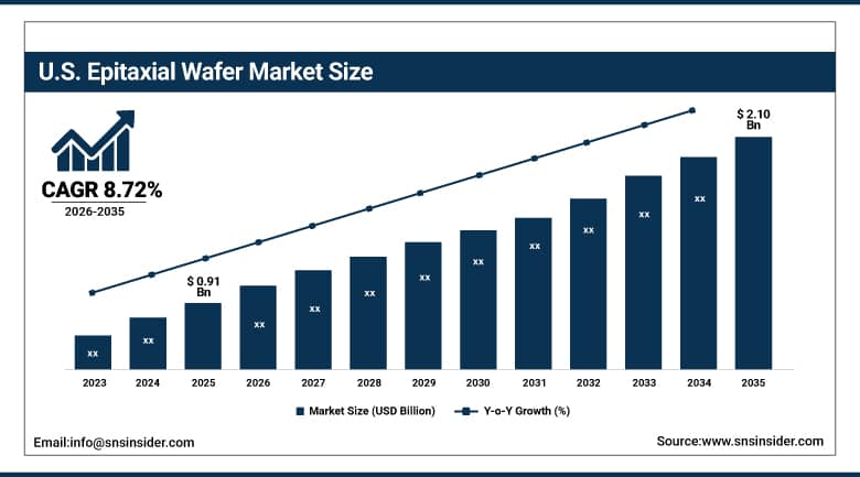
The U.S. epitaxial wafer market was valued at approximately USD 0.91 Billion in 2025 and is expected to reach approximately USD 2.10 Billion by 2035, growing at a CAGR of approximately 8.72%.
Growth in the U.S. market is driven by rising demand for sophisticated semiconductor technology across automotive, consumer products, aerospace, and defense industries. Despite the fact that there are a lot of emerging countries on the world stage which pose a great threat to the United States, America still holds a very prominent place when it comes to research and development in semiconductor technologies. Domestic chip manufacturing has been greatly supported by investments in it, and the popularity of the electric vehicle along with the development of AI and 5G infrastructure boosts epitaxial wafer demand in the USA.
In December 2024, the U.S. Commerce Department finalized $406 million in subsidies for GlobalWafers to expand silicon wafer production across facilities in Texas and Missouri. The initiative is designed to establish the first high-volume U.S. production of 300-millimeter wafers for advanced semiconductors and to expand silicon-on-insulator wafer output, a significant step toward reducing American dependence on overseas wafer production for critical semiconductor applications.
Epitaxial Wafer Market Segment Analysis
-
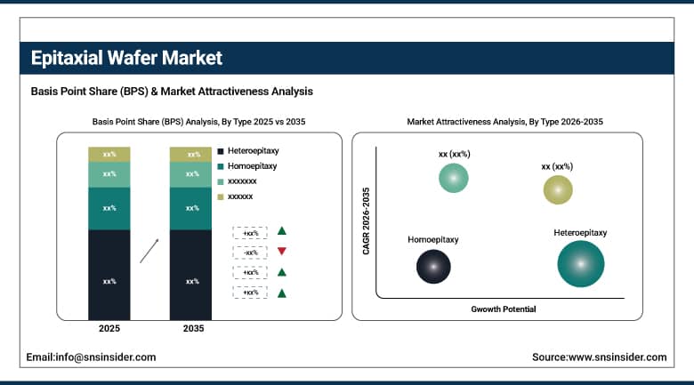
By Type, the heteroepitaxy segment dominated the epitaxial wafer market with a 59.60% revenue share in 2025, while the homoepitaxy segment is the fastest growing with a CAGR of approximately 12.43%.
-
By Wafer Size, the 9–12-inch segment dominated the epitaxial wafer market with a 53.71% revenue share in 2025, while the 5–8-inch segment is the fastest growing with a CAGR of approximately 14.45%.
-
By Application, the LED segment dominated the epitaxial wafer market with a 35.61% revenue share in 2025, while the power semiconductor segment is the fastest growing with a CAGR of approximately 13.00%.
-
By Industry Vertical, the consumer electronics segment dominated the epitaxial wafer market with a 42.30% revenue share in 2025, while the automotive segment is the fastest growing with a CAGR of approximately 14.29%.
By Type, heteroepitaxy dominates, homoepitaxy grows fastest
The Heteroepitaxy sub-segment of the global market for epitaxial wafers was estimated to contribute 59.60% of the overall market share of 2025, making it the largest among all the segments owing to its prominent usage in premium semiconductor products. IQE has dominated the industry in terms of innovation by manufacturing epitaxial wafers based on Gallium Arsenide and Gallium Nitride used in high-tech semiconductors including microLED and electro-optics, while the collaboration of Nexperia and Mitsubishi Electric on silicon carbide power semiconductors adds fuel to the fire.
Homoepitaxy is the most rapidly growing among the epitaxial growth techniques due to its good crystallinity and low density of defects, having a CAGR of around 12.43%. This trend is evidenced from the collaboration between Infineon Technologies and SK Siltron CSS to produce 150 mm silicon carbide wafers that are essential for high-voltage devices, and increasing demand for high-efficiency silicon carbide epitaxial wafers in solar cells by United Silicon Carbide, among others.
By Wafer Size, 9–12 inch dominates, 5–8 inch grows fastest
The leading wafer size segment during 2025 was the 9-12 inch segment, which accounted for 53.71% of the revenues, due to the common practice of using large-size wafers in high volume production of semiconductors, increasing efficiency and reducing costs. One of the key players in the segment is Siltronic AG, which manufactures 300mm silicon wafers in cooperation with Samsung Electronics in Singapore.
The 5-8 inch wafer size segment has been experiencing tremendous growth with an estimated CAGR of about 14.45% on account of increasing adoption of medium-sized wafers across applications such as MEMS devices, power semiconductors, and LEDs. IQE has diversified its manufacturing process and can now produce 8-inch gallium arsenide and gallium nitride wafers used in the fabrication of microLED and electro-optical devices.
By Application, LED dominates, power semiconductors grow fastest
The use of LED was dominant in the market during the year 2025 accounting for a revenue market share of 35.61%. The dominance is due to the widespread use of LED in the production of consumer electronic products, automotive lights, and lighting. The contribution of IQE to this dominance has been significant through the production of 8-inch gallium arsenide and gallium nitride epitaxial wafers.
The biggest use case for gallium nitride semiconductors is expected to be the power management segment, where it is forecasted to grow at a rate of 13.00% due to the increased need for effective power management in renewable energy, industry, and EVs. Firms such as Transphorm have been leading the charge in manufacturing high-performing power transistors made from gallium nitride semiconductors.
By Industry Vertical, consumer electronics dominates, automotive grows fastest
Consumer electronics was the key player in vertical industry demand in 2025, contributing 42.30% of the overall revenue owing to growing demands for sophisticated consumer electronics such as smartphones, tablets, and wearable electronics, which require intricate semiconductor devices. The success of IQE has greatly been achieved through the production of 8-inch gallium arsenide and gallium nitride epitaxial wafers for microLED displays and other applications in optoelectronics, whereas advances in consumer electronics keep stimulating the demand for epitaxial wafers.
Automotive is the fastest growing industry verticals, with a forecasted CAGR of around 14.29%, due to rising use of complex semiconductor devices in electric vehicles, self-driving cars, and in-car entertainment systems. The provision of silicon carbide epitaxial wafers for the inverter of the Lexus RZ battery electric vehicle by Resonac Corporation is an example of how epitaxial wafers are becoming increasingly important in today's automotive industry, as they contribute to increased fuel efficiency and range of the vehicles.
Regional Analysis
|
Region |
Major Country |
Share within Region, 2025 (%) |
|---|---|---|
|
North America |
United States |
83.0% |
|
Europe |
Germany |
24.0% |
|
Asia Pacific |
China |
41.0% |
|
Middle East & Africa |
UAE |
28.0% |
|
Latin America |
Brazil |
37.0% |
North America Epitaxial Wafer Market Insights
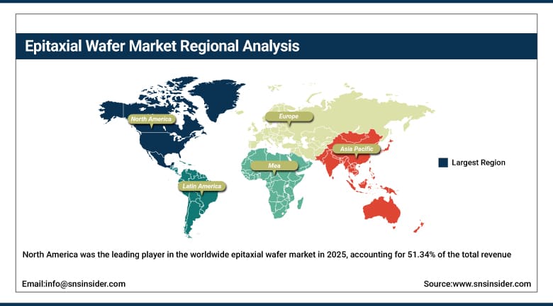
North America was the leading player in the worldwide epitaxial wafer market in 2025, accounting for 51.34% of the total revenue, as it had a robust semiconductor industry in the region and was actively investing in the production of electric vehicles, aerospace, and defense sector products. GlobalFoundries announced its partnership with General Motors for the manufacture of semiconductor chips in the United States.
Wolfspeed also opened a world-class silicon carbide production plant in Marcy, New York, with strong federal support, to address growing demand for power semiconductors in EVs and renewable energy technologies. These initiatives highlight North America's commitment to advancing semiconductor technology, reinforcing its position as the largest regional market for epitaxial wafers even as Asia Pacific grows faster in percentage terms.
Get Customized Report as Per Your Business Requirement - Enquiry Now
Europe Epitaxial Wafer Market Insights
Europe continues to be a technologically sound epitaxial wafer market, characterized by the strong presence of Germany as a hub for automobile and manufacturing industries that are becoming more reliant on silicon carbide and gallium nitride wafers. Siltronic AG, a company based out of Germany, holds a major share of the world manufacturing market for silicon wafers.
The European Chips Act will lead to further investment in fabrication and material for the region, where the EU is looking to cut its reliance on Asian and American supply chains of wafers. France, Italy, and the UK make up the other demands of the region, which will ensure continuous demand growth from automotive electrification and industrial automation.
Asia Pacific Epitaxial Wafer Market Insights
According to estimations, the Asia Pacific will experience the highest growth rate (CAGR), which will amount to approximately 14.63% during the forecast period (2035). This can be attributed to the growth witnessed in consumer electronics, IoT devices, and 5G network infrastructure. Specifically, LG Siltron has started the production of silicon carbide epilayer wafers of 6 inches in 2023 due to growing demands in power electronics, while United Silicon Carbide designed high-performance silicon carbide epitaxial wafers for solar cells.
These technological breakthroughs along with high investment in semiconductor fabrication facilities have made Asia Pacific a rising star in the global epitaxial wafers market. China, Japan, and South Korea are expanding their wafer fabrication capacities, and the government initiatives to ensure self-sufficiency in semiconductors will help the region maintain its growth rate above other regions.
MEA & Latin America Epitaxial Wafer Market Insights
The Middle East and Africa remain an early-stage epitaxial wafer market, with demand tied to growing electronics assembly and renewable energy infrastructure investment. In the region, the UAE dominates the market through its efforts to develop the capacity for solar energy generation as well as smart projects that involve power semiconductor devices, while Saudi Arabia seeks to invest in technological infrastructure in order to diversify its industries.
Latin America is seeing early but growing epitaxial wafer demand led by Brazil, where expanding electronics manufacturing and automotive production are creating new consumption of power semiconductor and LED-related wafers. Mexico follows as the region's second-largest market, benefiting from its role as an electronics and automotive assembly hub serving North American supply chains.
Market Dynamics
Growth Drivers: Advanced semiconductor materials in power electronics
One fact that needs to be taken into consideration is that the increased adoption of emerging advanced semiconductor materials like silicon carbide and gallium nitride in the industry of power electronics and automobiles is contributing towards the growth of the epitaxial wafers market. These semiconductors are known to have higher efficiency regarding thermal conductivity and voltage resistance. Since the demand for electric vehicles is increasing, governments are advocating cleaner transport means. Automakers are investing heavily in next-gen semiconductor technology using epitaxial layers.
Growth is also being fueled by consumer electronics and factory control systems, which need higher efficiency parts to be able to operate continuously with high frequency and power output. Governmental and commercial sectors are supporting research and development initiatives along with the construction of infrastructure to ramp up production of epitaxial wafers.
Restraints: High capital investment requirements limiting smaller players
The epitaxial wafer market requires heavy capital outlay to establish manufacturing facilities. The fabrication process uses advanced deposition methods, temperature controls and ultraclean environments which require a lot of money to be put in before production of even one single wafer can start.
Maintaining quality standards and yield efficiency across different wafer sizes adds further operational complexity and cost, which means most small and medium-sized businesses can't realistically access the market, leading to high concentration among a handful of large players. These cost barriers also limit innovation and scale in developing markets where semiconductor infrastructure funding tends to be scarce, and the long return-on-investment timeline in this category further discourages new market entrants.
Opportunities: Demand for epitaxial wafers in 5G infrastructure and smart devices
The wide implementation of 5G networks and rising adoption of smart devices are creating numerous growth avenues for the epitaxial wafer industry. In order to develop high frequency and high speed components for use in 5G base stations, RF front ends and smart sensors, epitaxial wafers become indispensable due to their excellent performance attributes.
The increasing global need for speedy and reliable connectivity will encourage telecom companies and original equipment manufacturers to upgrade to new infrastructure, thus increasing the demand for wafers. The smart home, industrial IoT, wearables, and self-guided technology require small and efficient chips manufactured on the epitaxial wafers, which presents an opportunity for wafer manufacturers to diversify their products.
Recent Developments:
-
2026: Wolfspeed, Inc. expanded silicon carbide epitaxial wafer production capacity to support growing demand from electric vehicles, renewable energy systems, and industrial power electronics.
-
2026: Coherent Corp. introduced next-generation gallium nitride (GaN) and silicon carbide (SiC) epitaxial wafer solutions designed for high-frequency communications and advanced power semiconductor applications.
-
2025: In September 2025, Wolfspeed announced the commercial launch of its 200-millimeter silicon carbide materials portfolio, including bare wafers and epitaxy, a major step toward scaling high-performance power device production.
Epitaxial Wafer Companies are:
-
SUMCO Corporation
-
Siltronic AG
-
Wolfspeed, Inc.
-
Coherent Corp.
-
IQE plc
-
IntelliEPI Inc.
-
SK Siltron Co., Ltd.
-
Resonac Corporation
-
Sumitomo Electric Industries, Ltd.
-
Nichia Corporation
-
Infineon Technologies AG
-
STMicroelectronics
-
Silicon Valley Microelectronics, Inc.
-
ASM International N.V.
-
Jenoptik AG
-
Mitsubishi Electric Corporation
-
onsemi
-
ROHM Co., Ltd.
Epitaxial Wafer Market Report Scope:
| Report Attributes | Details |
|---|---|
| Market Size in 2025 | USD 4.23 Billion |
| Market Size by 2035 | USD 11.93 Billion |
| CAGR | CAGR of 10.92% From 2026 to 2035 |
| Base Year | 2025 |
| Forecast Period | 2026-2035 |
| Historical Data | 2022-2024 |
| Report Scope & Coverage | Market Size, Segments Analysis, Competitive Landscape, Regional Analysis, DROC & SWOT Analysis, Forecast Outlook |
| Key Segments | • By Type (Heteroepitaxy, Homoepitaxy) • By Wafer Size (2–4 Inch, 5–8 Inch, 9–12 Inch, Others) • By Application (LED, Power Semiconductor, MEMS-Based Devices, Others) • By Industry Vertical (Consumer Electronics, Automotive, Healthcare, Industrial, Others) |
| Regional Analysis/Coverage | North America (US, Canada), Europe (Germany, UK, France, Italy, Spain, Russia, Poland, Rest of Europe), Asia Pacific (China, India, Japan, South Korea, Australia, ASEAN Countries, Rest of Asia Pacific), Middle East & Africa (UAE, Saudi Arabia, Qatar, South Africa, Rest of Middle East & Africa), Latin America (Brazil, Argentina, Mexico, Colombia, Rest of Latin America). |
| Company Profiles | GlobalWafers Co., Ltd., SUMCO Corporation, Siltronic AG, Wolfspeed, Inc., Coherent Corp., IQE plc, Soitec S.A., IntelliEPI Inc., SK Siltron Co., Ltd., Resonac Corporation, Sumitomo Electric Industries, Ltd., Nichia Corporation, Infineon Technologies AG, STMicroelectronics, Silicon Valley Microelectronics, Inc., ASM International N.V., Jenoptik AG, Mitsubishi Electric Corporation, onsemi, ROHM Co., Ltd. |

Frequently Asked Questions
The Epitaxial Wafer Market was valued at USD 4.23 Billion in 2025.
Heteroepitaxy dominated with a 59.60% revenue share in 2025.
North America dominated the Epitaxial Wafer Market in 2025 with approximately 51.34% market share.
Rising demand for advanced electronics, electric vehicles, and 5G technology, all of which depend on the higher device efficiency and reliability that epitaxial wafers enable.
The Epitaxial Wafer Market is expected to grow at a CAGR of 10.92% from 2026 to 2035.
