Interposer and Fan-out Wafer Level Packaging Market Size Analysis:
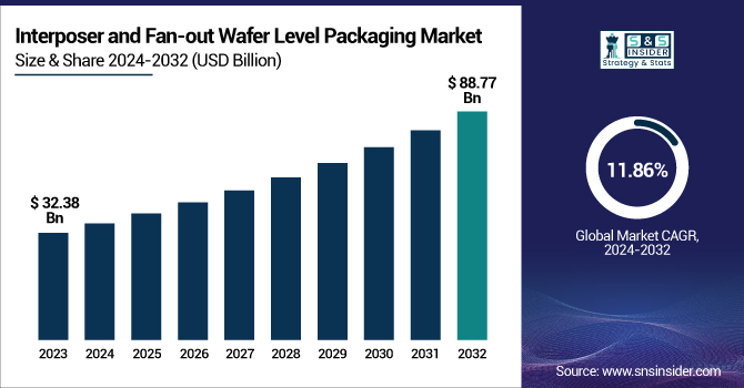
The Interposer and Fan-out Wafer Level Packaging Market was valued at USD 32.38 billion in 2023 and is projected to reach USD 88.77 billion by 2032, growing at a CAGR of 11.86% from 2024 to 2032.
To Get more information on Interposer and Fan-out Wafer Level Packaging Market - Request Free Sample Report
Key drivers include the rising demand for high-performance computing (HPC), AI, 5G, and IoT devices, along with the push for miniaturization and enhanced thermal efficiency. Adoption rates are accelerating due to cost-efficient production and improved yield rates, while sustainability efforts focus on reducing material waste and power consumption. Cost reduction trends, such as eliminating substrates in FOWLP, enhance reliability, making it a preferred choice over traditional packaging. The U.S. leads in patent filings and R&D investments, driving innovations in advanced semiconductor packaging. In the U.S. market, it was valued at USD 8.47 billion in 2023 and is expected to reach USD 19.99 billion by 2032, expanding at a CAGR of 10%.
Interposer and Fan-out WLP Market Dynamics:
Drivers:
-
Surging Demand for AI and Cloud Computing Drives Advanced Packaging Growth
The Interposer and Fan-out Wafer Level Packaging Market is growing rapidly, fueled by the increasing demand for AI, cloud computing, and data centers. Companies like TSMC and Synopsys are leading advancements in Chip-on-Wafer-on-Substrate (CoWoS) and Integrated Fan-Out (InFO) technologies, optimizing chip performance and reducing power consumption. The active interposer method enhances 3D-stacked chiplet integration, lowering power usage by 30% while boosting computational efficiency. The surge in AI accelerators, GPUs, and networking chips has contributed to a 20% stock rise for Camtek, reflecting strong market growth. Additionally, 3D packaging innovations are cutting latency, increasing bandwidth, and enabling higher transistor density. With rising adoption in automotive, IoT, and edge computing, the need for cost-effective, high-speed semiconductor packaging continues to accelerate, making advanced packaging crucial for next-generation electronics.
Restraints:
-
The complexity of 3D-stacked chiplets and heterogeneous integration raises alignment, thermal, and signal challenges, reducing yield and increasing costs.
The increasing adoption of 3D-stacked chiplets and heterogeneous integration presents significant design and manufacturing challenges in the Interposer and Fan-out Wafer Level Packaging Market. Achieving precise alignment, efficient thermal management, and robust signal integrity is crucial for ensuring high performance and reliability. However, warpage, stress-induced defects, and electrical interference often lead to lower production yields, increasing costs for manufacturers. Additionally, variations in material properties and interconnect densities complicate the fabrication process, requiring advanced lithography, wafer bonding, and testing techniques. As devices become smaller and more powerful, maintaining high-speed data transfer while minimizing power loss remains a key hurdle. To overcome these challenges, companies are investing in AI-driven design automation, new interposer materials, and improved testing methodologies, yet the complexity of integration continues to be a critical restraint for scalability and mass production.
Opportunities:
-
Revolutionizing Semiconductor Packaging with 3D Integration
The evolution of 3D stacking, chiplet architectures, and hybrid bonding is revolutionizing semiconductor packaging, enabling higher performance, reduced power consumption, and greater miniaturization. These innovations combine several dies within one package to increase bandwidth, minimize latency, and improve thermal performance, making them perfect for AI, high-performance computing (HPC), and data centers. Hybrid bonding enables tighter intermolecular connections, improving signal integrity at a given pitch and reducing resistance and power loss. Heterogeneous integration also enables the integration of logic, memory, and RF components, which optimizes system performance as well. With both compact and high-speed computing on the rise, no-doubt foundries and open-source advanced technology (OSATs) have invested heavily to create the next generation of advanced packaging solutions to deliver high-density, energy-efficient semiconductor devices.
Challenges:
-
Supply chain bottlenecks in advanced packaging arise from material shortages, trade restrictions, and limited availability of high-purity substrates.
The Interposer and Fan-out Wafer Level Packaging Market faces challenges due to its reliance on high-purity materials, advanced lithography tools, and specialized substrates, leading to supply chain bottlenecks and increased lead times. The scarcity of key raw materials like silicon interposers and high-performance resins impacts production efficiency and cost. Additionally, geopolitical tensions, trade restrictions, and capacity constraints in semiconductor fabrication further strain availability. To mitigate risks, manufacturers are diversifying suppliers, investing in local production facilities, and adopting alternative materials, but overcoming these hurdles remains a critical industry challenge.
Interposer and Fan-out Wafer Level Packaging Industry Segment Analysis:
By Packaging Component & Design
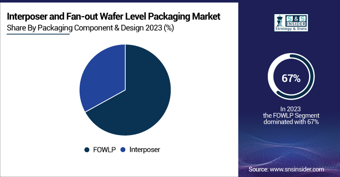
The Fan-out Wafer Level Packaging (FOWLP) segment dominated the Interposer and Fan-out Wafer Level Packaging Market in 2023, accounting for approximately 67% of total revenue. Its widespread adoption is driven by superior performance, reduced form factor, and enhanced thermal efficiency, making it a preferred choice for high-performance computing (HPC), AI processors, and 5G applications. Compared to traditional packaging, FOWLP eliminates the need for an interposer, reducing costs while improving electrical and thermal characteristics. Major industry players like TSMC, ASE Group, and Amkor Technology continue to invest in innovative fan-out solutions to support the growing demand for advanced semiconductors in consumer electronics, automotive, and data centers. With increasing integration of chiplets and heterogeneous architectures, FOWLP is expected to maintain its leadership position, driving innovation in next-generation semiconductor packaging.
The Interposer segment is projected to be the fastest-growing in the Interposer and Fan-out Wafer Level Packaging Market from 2024 to 2032, driven by increasing demand for 3D-stacked chiplets, high-bandwidth memory (HBM), and heterogeneous integration. Interposers enhance signal integrity, power efficiency, and miniaturization, making them essential for AI, cloud computing, and HPC applications. Leading semiconductor manufacturers like TSMC, Intel, and Samsung are accelerating advancements in silicon interposers and glass-based substrates to support next-generation processors and GPUs. Additionally, increasing adoption in data centers, 5G infrastructure, and advanced automotive electronics is fueling growth. With scalability, improved thermal performance, and enhanced bandwidth, the Interposer segment is set to experience significant expansion, playing a critical role in the future of semiconductor packaging.
By Packaging
The 2.5D packaging segment dominated the Interposer and Fan-out Wafer Level Packaging Market in 2023, holding approximately 58.9% of total revenue. This dominance is driven by high demand for advanced semiconductor integration in AI, HPC, and networking applications. 2.5D architectures offer superior performance, power efficiency, and scalability by integrating HBM, GPUs, and ASICs on a single interposer. Major players like TSMC, AMD, and Intel leverage silicon interposers to enhance bandwidth, signal integrity, and thermal management, making it a preferred solution for data centers and high-performance applications. Additionally, 2.5D packaging reduces latency and improves interconnect density, catering to the increasing need for miniaturization and heterogeneous integration. With continued innovation in chiplet-based designs and hybrid bonding, 2.5D packaging is expected to maintain a strong market presence, shaping the future of advanced semiconductor manufacturing.
The 3D packaging segment is expected to be the fastest-growing in the Interposer and Fan-out Wafer Level Packaging Market from 2024 to 2032, In contrast to 2.5D architectures, where interconnects must traverse silicon and die to the silicon interface, 3D packaging allows for almost direct die-to-die interconnects, which also enables lower power consumption, higher bandwidth, and faster processing. Driving this growth are the increasing demand for AI accelerators, high-performance computing (HPC), and advanced data center processors. Key semiconductor players including Intel, TSMC, and Samsung have been investing significantly into 3D integration for next-generation AI chips, edge computing, and autonomous systems. 3D packaging also increases miniaturization and system efficiency, thus making it one of the key technologies for future semiconductors. As we push the limits of computing, 3D architectures will be integral in defining the next era of chip innovation.
By Devices Type
The Logic ICs segment led the Interposer and Fan-out Wafer Level Packaging Market in 2023, accounting for approximately 38% of total revenue. This dominance is driven by the rising demand for AI processors, high-performance computing (HPC), and advanced system-on-chip (SoC) solutions. Logic ICs, including CPUs, GPUs, and AI accelerators, require high-density interconnects, improved thermal management, and power efficiency, making advanced packaging technologies like 2.5D and 3D integration essential. Key industry players such as Intel, AMD, NVIDIA, and TSMC are investing in chiplet-based architectures and heterogeneous integration to enhance performance. With the continued growth of cloud computing, edge AI, and data centers, the Logic ICs segment is expected to maintain its dominance, driving innovation and efficiency in next-generation semiconductor designs.
The LEDs segment is projected to witness significant growth in the Interposer and Fan-out Wafer Level Packaging Market from 2024 to 2032. This expansion is driven by the increasing demand for miniLED and microLED displays in consumer electronics, automotive lighting, and advanced display technologies. High-efficiency, compact form factors, and enhanced thermal performance are critical factors accelerating the adoption of fan-out wafer-level packaging (FOWLP) and 3D integration for LEDs. Companies like Samsung, Apple, and Osram are investing in next-generation LED solutions, leveraging advanced packaging to improve brightness, durability, and energy efficiency. The rapid growth of smartphones, wearables, AR/VR devices, and high-resolution displays further fuels this trend. With ongoing innovations in chip-scale packaging (CSP) and wafer-level optics, the LEDs segment is poised to become a key driver in the advanced semiconductor packaging landscape.
By End-User
The communication segment dominated the Interposer and Fan-out Wafer Level Packaging Market in 2023, accounting for approximately 30% of total revenue. This dominance is driven by the rising adoption of 5G networks, high-speed data transmission, and cloud computing. The increasing demand for low-latency, high-bandwidth communication infrastructure has fueled the integration of advanced packaging solutions in networking equipment, base stations, and optical transceivers. Key players like Qualcomm, Broadcom, and Intel are investing in fan-out wafer-level packaging (FOWLP) and 2.5D/3D integration to enhance signal integrity, power efficiency, and miniaturization. Additionally, the rapid expansion of data centers, IoT devices, and satellite communications has further accelerated the need for high-performance computing (HPC) solutions. As the global telecom industry continues to evolve, advanced packaging technologies will remain critical in enabling next-generation connectivity solutions.
The medical devices segment is projected to be the fastest-growing in the Interposer and Fan-out Wafer Level Packaging Market from 2024 to 2032, due to the advancements in miniaturized medical electronics, wearable health monitoring devices, and implantable sensors. The growing integration of AI-enabled clinical diagnostic tools, telemedicine and smart biosensors has increased the demand for high-performance, energy-efficient semiconductor packaging. Medical Equipment as an end-product make use of 2.5D and 3D integration technologies for advanced uses: Med-chips to enhance various microelectronics like medical imaging equipment, portable diagnostic devices, and neuro stimulators introduce it for high power efficiency and signal integrity. Minimally invasive, high-performance medical devices are being developed and there are several companies LIKE Medtronic, Philips, GE Healthcare investing in heterogeneous integration and fan-out wafer-level packaging (FOWLP). Whether it is precision medicine, remote patient monitoring, or AI-powered healthcare innovations, advanced semiconductor packaging will be a key driver in changing the dynamics of next-gen medical technology.
Interposer and Fan-out WLP Market Regional Outlook:
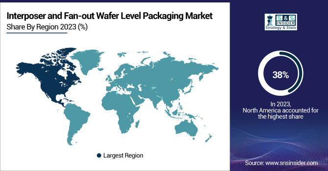
North America led the Interposer and Fan-out Wafer Level Packaging Market in 2023, accounting for 38% of total revenue, driven by the strong presence of semiconductor giants such as Intel, AMD, Broadcom, and Qualcomm. The region's leadership is fueled by high investments in advanced semiconductor packaging technologies, increasing demand for AI, HPC, and cloud computing, and a well-established supply chain. Additionally, government initiatives such as the CHIPS Act are boosting domestic semiconductor manufacturing, further strengthening North America’s dominance. The growing adoption of 5G, autonomous vehicles, and medical devices is accelerating demand for high-performance, miniaturized semiconductor solutions. With continuous advancements in heterogeneous integration, 3D packaging, and fan-out wafer-level packaging (FOWLP), North America is expected to maintain its market leadership in the coming years.
Asia-Pacific is projected to be the fastest-growing region in the Interposer and Fan-out Wafer Level Packaging Market from 2024 to 2032, driven by rising demand for AI, IoT, and 5G applications, as well as solid governmental support. China, Taiwan, South Korea and Japan rank first in the packaging of semiconductor innovations, with TSMC, Samsung, and ASE Group investing heavily in advanced packaging technologies. India has a strong consumer electronics ecosystem, at a low production cost, supported by a growing consumer electronics market. Government initiatives such as China’s "Made in China 2025" and India’s semiconductor incentive programs are further driving growth. With the growing demand for miniaturized and high-performance chips, Asia Pacific is poised to grow faster than any other region in terms of market growth, setting it as the pivotal center for next-generation semiconductor packaging technologies.
Get Customized Report as per Your Business Requirement - Enquiry Now
Key Players Listed in Interposer and Fan-out Wafer Level Packaging Market are:
-
Samsung Electronics (South Korea) – Advanced packaging solutions, 2.5D/3D ICs, high-density interposers
-
Taiwan Semiconductor Manufacturing Company Ltd. (Taiwan) – Foundry services, CoWoS, InFO packaging
-
SK HYNIX INC. (South Korea) – Memory chips, DRAM, NAND Flash
-
Intel Corporation (U.S.) – Processors, 3D packaging, Foveros technology
-
United Microelectronics Corporation (Taiwan) – Foundry services, semiconductor packaging
-
Toshiba Corporation (Japan) – Storage solutions, advanced semiconductor packaging
-
Powertech Technology Inc. (Taiwan) – Semiconductor assembly and testing services
-
Siliconware Precision Industries Co. Ltd. (Taiwan) – IC packaging and assembly services
-
Qualcomm Technologies Inc. (U.S.) – Mobile chipsets, RF front-end solutions
-
Murata Manufacturing Co. Ltd. (Japan) – Electronic components, module packaging
-
ALLVIA, Inc. (U.S.) – 3D interconnects, TSV technology
-
AMETEK Inc. (U.S.) – Electronic instruments, interconnects
-
Amkor Technology (U.S.) – OSAT services, fan-out wafer-level packaging (FOWLP)
-
ASE Technology Holding Co., Ltd. (Taiwan) – Semiconductor packaging, SiP, FOWLP
-
ASTI Holdings Limited (Singapore) – Semiconductor testing, assembly solutions
-
Broadcom (U.S.) – Networking, RF, optical semiconductor solutions
-
Infineon Technologies AG (Germany) – Power semiconductors, automotive chips
-
LAM RESEARCH CORPORATION (U.S.) – Semiconductor manufacturing equipment
-
STMicroelectronics (Switzerland) – Analog, MEMS, power semiconductors
-
Texas Instruments Incorporated (U.S.) – Analog ICs, power management chips
List of key suppliers providing raw materials and components for the Interposer and Fan-out Wafer Level Packaging Market:
-
Soitec (France)
-
Ajinomoto Fine-Techno (Japan)
-
Hitachi Chemical (Japan)
-
Nagase ChemteX Corporation (Japan)
-
Veeco Instruments Inc. (USA)
-
Shin-Etsu Chemical Co., Ltd. (Japan)
-
Dow Inc. (USA)
-
DuPont (USA)
-
JSR Corporation (Japan)
-
Sumitomo Bakelite Co., Ltd. (Japan)
-
Toray Industries, Inc. (Japan)
-
BASF SE (Germany)
-
Mitsui Chemicals, Inc. (Japan)
-
Henkel AG & Co. KGaA (Germany)
-
Showa Denko K.K. (Japan)
| Report Attributes | Details |
|---|---|
| Market Size in 2023 | USD 32.38 Billion |
| Market Size by 2032 | USD 88.77 Billion |
| CAGR | CAGR of 11.86% From 2024 to 2032 |
| Base Year | 2023 |
| Forecast Period | 2024-2032 |
| Historical Data | 2020-2022 |
| Report Scope & Coverage | Market Size, Segments Analysis, Competitive Landscape, Regional Analysis, DROC & SWOT Analysis, Forecast Outlook |
| Key Segments | • By Packaging Component & Design(Interposer, FOWLP) • By Packaging Type(2.5D, 3D) • By Devices Type(Logic ICs, Imaging & Optoelectronics, LEDs, MEMS/Sensors, Memory Devices, Others) • By End-User(Communication, Manufacturing, Medical Devices, Consumer Electronics, Automotive, Aerospace) |
| Regional Analysis/Coverage | North America (US, Canada, Mexico), Europe (Eastern Europe [Poland, Romania, Hungary, Turkey, Rest of Eastern Europe] Western Europe] Germany, France, UK, Italy, Spain, Netherlands, Switzerland, Austria, Rest of Western Europe]), Asia Pacific (China, India, Japan, South Korea, Vietnam, Singapore, Australia, Rest of Asia Pacific), Middle East & Africa (Middle East [UAE, Egypt, Saudi Arabia, Qatar, Rest of Middle East], Africa [Nigeria, South Africa, Rest of Africa], Latin America (Brazil, Argentina, Colombia, Rest of Latin America) |
| Company Profiles | Samsung Electronics (South Korea), Taiwan Semiconductor Manufacturing Company Ltd. (Taiwan), SK HYNIX INC. (South Korea), Intel Corporation (U.S.), United Microelectronics Corporation (Taiwan), Toshiba Corporation (Japan), Powertech Technology Inc. (Taiwan), Siliconware Precision Industries Co. Ltd. (Taiwan), Qualcomm Technologies Inc. (U.S.), Murata Manufacturing Co. Ltd. (Japan), ALLVIA, Inc. (U.S.), AMETEK Inc. (U.S.), Amkor Technology (U.S.), ASE Technology Holding Co., Ltd. (Taiwan), ASTI Holdings Limited (Singapore), Broadcom (U.S.), Infineon Technologies AG (Germany), LAM RESEARCH CORPORATION (U.S.), STMicroelectronics (Switzerland), Texas Instruments Incorporated (U.S.). |
Frequently Asked Questions
North America dominated the Interposer and Fan-out Wafer Level Packaging Market in 2023.
The “FOWLP” segment dominated the Interposer and Fan-out Wafer Level Packaging Market.
Increasing demand for high-performance computing, miniaturization of electronic devices, 5G adoption, AI advancements, and rising semiconductor packaging innovation.
The Interposer and Fan-out Wafer Level Packaging Market was USD 32.38 Billion in 2023 and is expected to reach USD 88.77 Billion by 2032.
The Interposer and Fan-out Wafer Level Packaging Market is expected to grow at a CAGR of 11.86% during 2024-2032.
Get in Touch
