Panel Level Packaging Market Size & Growth Trends:
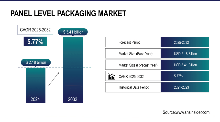
The Panel Level Packaging Market size was valued at USD 2.18 billion in 2024 and is expected to reach USD 3.41 billion by 2032, growing at a CAGR of 5.77% over the forecast period 2025-2032.
To Get more information on Panel Level Packaging Market - Request Free Sample Report
The increasing demand for high performance, miniaturized semiconductor devices, increased instruction from AI, 5G, and automotive electronics, the need for cost-efficient packaging solutions, and the transition to heterogeneous integration and multi-die packaging are the major factors driving the growth of the Panel Level Packaging market.
The growth of the Panel Level Packaging (PLP) market is majorly attributed to the growing complexity of semiconductor devices and demand for high-performance packaging solutions. PLP is a low-cost, high-density packaging solution that is also scalable, making it easy to combine several dies/memory and other chips on a single panel. LAP has proven useful for many applications such as AI, 5G, automotive electronics, and mobile packages.
According to a 2023 paper published in the Journal of Microelectronics and Electronic Packaging, PLP has been the "most suited" packaging solution for 5G RF modules and AI accelerators due to its capacity for both high-frequency operations and thermal management.
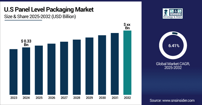
The U.S. Panel Level Packaging Market is estimated to be USD 0.33 billion in 2024 and is projected to grow at a CAGR of 6.41%. The growing demand for low-cost and highly scalable solutions with the value-added capabilities of PLP technology in the high-performance computing (HPC), IoT device & medical electronics industries, driven by a growing need for flexibility along with increased investments in advanced manufacturing technologies, is driving the U.S. PLP market.
Panel Level Packaging Market Dynamics
Key Drivers:
- Driving Growth in Panel Level Packaging with Cost-Effective High-Performance Solutions
The demand for cost-effective, high-performance packaging solutions in compact form factors is driving the Panel Level Packaging market. As devices shrink and become more complicated, conventional packaging is limited by performance, scale, and cost. The ability to use PLP, allowing for the larger substrate format and more dies per panel, helps lower the overall costs to manufacture while still advancing device functionality.
Data from Yole Group indicates the quick industrial adoption of PLP, in which more than 500 million PLP-based packages were shipped in 2023.
Restrain:
- Overcoming Technological Complexities and Standardization Challenges in Panel Level Packaging
The major hurdle to overcome in the PLP market is the technological complexities in the handling of the panel, as well as the warpage control issue. Compared to larger panel substrates, wafer-level formats are significantly less susceptible to mechanical deformation during processing, resulting in defects and low yield. A huge amount of equipment and materials innovation is needed to ensure accurate alignment, control differences in thermal expansion, and deposit layers uniformly, even on large panels. There is still no industry-wide standardization of panel sizes, processes, and materials, which leads to interoperability issues across equipment vendors and slows the development of the ecosystem.
As reported by TechSearch International, panel warpage accounts for more than 30% of process-related yield loss for PLP pilot lines at the early stages of manufacturing
Opportunity:
- Unlocking Panel Level Packaging Potential in Automotive HPC and Advanced Technology Applications
PLP's best opportunity is in automotive and high-performance computing (HPC), where the I/O density needed in tier 1 systems to integrate ADAS, EV, and HPC at the processor level creates a powerful need for PLP's thermal efficiency. Importantly, glass and composite carrier material advancements are opening up new horizons in high-frequency and optical applications, expanding the scope of the technology. TSMC and Samsung are leading the way in panel-based packaging to enable the scaling of 2.5D/3D integration.
SEMI reported that total worldwide spending on advanced packaging facilities exceeded USD 8 billion in 2023, emphasizing PLP's strategic significance.
Challenges:
- Overcoming Infrastructure Limitations and Ecosystem Immaturity to Accelerate Panel Level Packaging
The infrastructure limitations and the immaturity of the ecosystem are also other crucial restrictions. Wafer-level technologies have matured over decades and have reached a relative maturity. Thanks to tool cross-stacking, PLP does not have such a robust supply chain, and tooling has not reached a wide range of similar specifications. But large substrates require scalable solutions from equipment suppliers for processes such as die placement, molding, and panel singulation. Additionally, not having broad foundry and OSAT participation at full production scale limits the speed of commercialization.
According to the 2023 SEMI Equipment report, industrial readiness for PLP is very low, with fewer than 10 pilot or production-scale PLP facilities in the world.
Panel Level Packaging Market Segments Analysis
By Technology Type
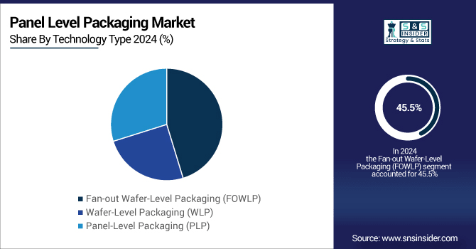
Fan-out Wafer-Level Packaging (FOWLP) had the largest stake in the market in 2024, seizing 45.5% share of the market, largely because of its popularity roots with mobile and consumer electronics. The combination of small footprint, efficient packaging, high performance, and low-profile packaging without the need for substrates makes it especially suited to devices with demanding thermal and high electrical performance requirements.
Panel-Level Packaging (PLP) is predicted to be the fastest-growing technology from 2025 to 2032, owing to its capability of processing larger formats and thereby driving down the cost per unit dramatically. The industry interest is growing across AI, automotive, and high-performance computing applications, as PLP not only scales to fit within processor systems but also works in combination with 2.5D and 3D integration types. PLP is set to shake up advanced packaging.
By Carrier Type
The largest market share was held by Rigid Carriers in 2024, accounting for 37.5% of the total due to their high utilization in mainstream semiconductor packaging processes Such carriers provide good mechanical stability alongside compatibility with mature manufacturing lines, meaning that they are commonly used in many high-volume applications on consumer electronics, telecommunications, and industrial devices. Rigid carriers (mainly on silicon or ceramics) maintain support for important applications where mechanical stability and established reliability are crucial.
Composite Carriers is expected to grow at the highest rate from 2025 to 2032. For emerging high-density and heterogeneous integration, they provide excellent mechanical and thermal properties as well as high electrical performance by exploiting the combination of different types of materials. In AI, automotive electronics, and 5G devices, the composite carriers are especially suited. As R&D investments increase and demand for more customizable packaging substrates ramps up, composite carriers are quickly stepping into the focus of advanced packaging innovators and fabs across the globe.
By Carrier Type
The panel-level packaging market was dominated by Consumer Electronics in 2024, representing 41.4% of the total share. This is primarily driven by the high adoption of advanced packaging in the automotive sector, particularly in smartphones, tablets, laptops, and wearable devices. For these high-volume products, panel-level packaging allows the density, performance, and efficiency that is needed. As the integration of 5G and IoT continues, PLP is preferred by major consumer tech companies and foundries to meet the growing performance-per-watt and form factor demand of devices.
Due to the global transition to electric vehicles (EVs), autonomous driving technologies, and advanced driver-assistance systems (ADAS), Automotive Electronics is projected to experience the fastest CAGR from 2025 to 2032. PLP shines in these applications, where strong, thermally efficient, and high-density packaging is required. The demand for next-gen packaging solutions, driven primarily by the automotive sector for reliability and performance in harsh environments, will position PLP as a central enabler of future mobility systems.
Panel Level Packaging Market Regional Outlook
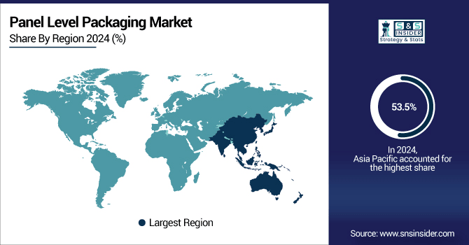
Asia Pacific leading regional PLP market in 2024, commanding a 53.5% share due to robustness in semiconductor manufacturing and capacity for high-volume production. It hosts some of the largest foundries and outsourced semiconductor assembly and test (OSAT) suppliers in the world, including TSMC, ASE, JCET, and others. These guys have been deploying PLP for consumer electronics and mobile devices. Also, regional governments have aided semiconductor expansion using tax breaks and investment.
Taiwan dominates the regional landscape with its leading packaging technology, partially thanks to TSMC, the world's largest and one of the most advanced packaging innovators.
North America will continue to see the fastest CAGR during the 2025-2032 period, driven mainly by automotive electronics, AI, and high-performance computing (HPC) applications. Prominent figures continued to stake their claims: U.S.-based titans such as Intel and Amkor are investing big money in panel-based packaging R&D and infrastructure as a means of shoring up a domestic semiconductor ecosystem. The growth is also fueled by the semiconductor independence affirmation and the CHIPS Act.
The US, with its mature R&D ecosystem and government support, remains dominant in North America with technological leadership in advanced chip design and packaging innovation.
Europe has been slowly growing and gaining more interest in the Panel-Level Packaging (PLP) market thanks to its automotive and industrial electronics demand. A: It focuses on ruggedness and high-level integration for extreme environmental conditions.
With its relatively much stronger automotive industry and key companies such as Infineon and Bosch promoting PLP for EVs, ADAS, and power electronics applications Germany is the lead country.
Latin America and the Middle East & Africa hold a minimal share of the Panel Level Packaging market owing to very little semiconductor manufacturing infrastructure growth in the regions. Regions dependent on imports and in the early stages of adoption of advanced packaging technologies with more potential for growth in conjunction with future industrial and digital transformation efforts.
Get Customized Report as per Your Business Requirement - Enquiry Now
Key Players Listed in the Panel Level Packaging Market are:
Some of the major key players are ASE Group, Amkor Technology, TSMC, Samsung Electronics, JCET Group, Nepes Corporation, PTI, Deca Technologies, Intel, SPIL and others.
Recent Development
-
In February 2025, ASE and PTI are ramping up investments in Fan-Out Panel-Level Packaging (FOPLP) to meet surging AI and HPC chip demand.
-
In June 2024, Samsung Electronics entered the Panel-Level Packaging (PLP) market ahead of TSMC, advancing Fan-Out PLP for large AI chips. Leveraging early investments and experience with plastic panels, Samsung aims to lead in scalable AI packaging solutions.
| Report Attributes | Details |
|---|---|
| Market Size in 2024 | USD 2.18 Billion |
| Market Size by 2032 | USD 3.41 Billion |
| CAGR | CAGR of 5.77% From 2025 to 2032 |
| Base Year | 2024 |
| Forecast Period | 2025-2032 |
| Historical Data | 2021-2023 |
| Report Scope & Coverage | Market Size, Segments Analysis, Competitive Landscape, Regional Analysis, DROC & SWOT Analysis, Forecast Outlook |
| Key Segments | • By Technology Type (Fan-out Wafer-Level Packaging (FOWLP), Wafer-Level Packaging (WLP), Panel-Level Packaging (PLP)) • By Carrier Type (Rigid Carrier, Flexible Carrier, Organic Substrate Carrier, Glass Carrier, Metal Carrier, Composite Carrier) • By End User (Consumer Electronics, Automotive Electronics, Telecommunications, Industrial Electronics, Healthcare Devices, Others) |
| Regional Analysis/Coverage | North America (US, Canada, Mexico), Europe (Germany, France, UK, Italy, Spain, Poland, Turkey, Rest of Europe), Asia Pacific (China, India, Japan, South Korea, Singapore, Australia, Rest of Asia Pacific), Middle East & Africa (UAE, Saudi Arabia, Qatar, South Africa, Rest of Middle East & Africa), Latin America (Brazil, Argentina, Rest of Latin America) |
| Company Profiles | ASE Group, Amkor Technology, TSMC, Samsung Electronics, JCET Group, Nepes Corporation, PTI, Deca Technologies, Intel, SPIL. |
Get in Touch
