High-K Dielectric Material Market Size & Trends:
The High-K Dielectric Material Market size was valued at USD 1.67 billion in 2024 and is projected to reach USD 3.75 billion by 2032, growing at a CAGR of 10.63% during 2025-2032.
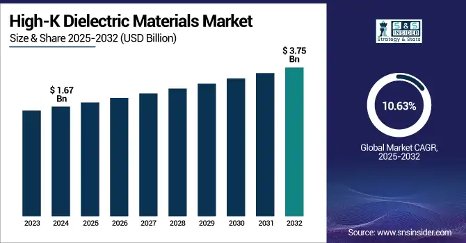
To Get more information on High-K dielectric materials Market - Request Free Sample Report
The high-k dielectric materials market refers to the industry involved in the development, production, and distribution of advanced dielectric materials with high dielectric constants (K-values) used in semiconductor device fabrication. These materials are critical for replacing traditional insulators in transistor structures to enable enhanced electrical performance, reduced power consumption, and continued scaling in integrated circuits. They are widely used in logic chips, memory devices, and emerging technologies, applied through processes including Atomic Layer Deposition (ALD). The market is driven by rising demand for miniaturized, high-speed, and low-power electronics across various applications including consumer devices, automotive electronics, and artificial intelligence. It encompasses a broad network of raw material providers, chemical companies, and semiconductor manufacturers supporting innovation in chip design.
Murata Manufacturing and NIMS generated the world’s largest electronic materials database by collecting data from more than 20,000 material samples used in 5,000 academic publications. Their AI-driven screening sorted materials into seven ferroelectric families to accelerate the discovery of new electronic materials.
The U.S. high-k dielectric materials market size was valued at USD 0.26 billion in 2024 and projected to reach USD 0.63 billion by 2032 expanding at a CAGR of 11.67%. Increasing use of advanced semiconductor devices and miniaturization of transistors in new technology nodes, such as 5nm and 7nm are the key factors that are fueling the growth of advanced packaging market. Application of microprocessor is driving the market due to the increasing demand for better performance, lower power consumption, and higher device density are rising requirement of logic chip, memory device, and energy-efficient electronic. With these technology advancements, the high-k gate dielectric materials becomes necessary to address gate leakage, device performance improvement and to meet the ensuring demands for such materials in the U.S. markets.
High-K Dielectric Material Market Dynamics:
Drivers:
-
High K Dielectric Materials Drive Performance in Advanced Semiconductor Nodes
As semiconductor devices continue to shrink to smaller nodes, such as 5nm and 3nm, the need for high-k dielectric materials becomes increasingly critical. These materials play a vital role in reducing gate leakage and improving the overall performance of advanced chips. High-k dielectrics material market growth is driven by their higher permittivity that enables the use of a thinner insulating layer while providing better performance, and reduces the risk of leakage, which can otherwise reduce the effectiveness of smaller transistors. This decrease is fueled by the increasing need for faster and more efficient electronic devices, particularly in applications such as mobile phones, AI and data centers. The ability of high-k dielectrics to support smaller transistor nodes without sacrificing performance is essential for meeting these evolving technological demands.
Applied Materials has introduced the first high-volume use of ruthenium for 2nm node chips, reducing resistance by 25%, and developed a new low-k dielectric material to enhance energy efficiency in AI computing.
Restraints:
-
Thermal Expansion Interface Mismatch and Compatibility Issues Limit High K Dielectric Adoption
High-k dielectric materials, while essential for advanced semiconductor nodes, may not always be compatible with all semiconductor materials, which can limit their adoption in certain applications. This compatibility problem is due to the specific characteristics of high-k materials, which are not compatible with previous properties of semiconductors, especially in the case of propagating technologies. Due to the progress of semiconductor technology, incorporation of these materials in current infrastructure could be even more problematic since it will require substantial modifications of manufacturing processes. For instance, differences in thermal expansion, mismatch in interface compatibility, or in electrical characteristics can cause a decrease in performance and more perversely reliability of old devices. Accordingly, use of high-k materials on a widespread basis is limited, especially in systems implemented using older semiconductor technologies that have not been tailored for such advanced materials.
Opportunities:
-
Advancements in 2D Materials and High-K Dielectrics Fuel Semiconductor Market Innovation
The integration of advanced 2D materials including hexagonal boron nitride (h-BN) and transition metal dichalcogenides (TMDs) in semiconductor devices is driving innovation in the high-k dielectric materials market. These compounds enable the growth of front-end-of-line (FEOL) and back-end-of-line (BEOL), which are essential for increasing carrier mobility and improving electrostatic control in transistors in order to ensure the performance of high-performance applications, such as AI and energy-efficient electronics. While its “natural enemy,” crystal growth, and the problem of doping control remain as challenges, the accelerating trend of heterogeneous integration and new materials’ development has opened up larger market segments, such as in smaller, higher power chips. This evolution is underpinning the growth of the high-k dielectric materials market, which is driving demand for more advanced chips in high-performing computing, energy-efficient electronics, and AI-driven technologies, providing great opportunity for market growth.
The next generation of semiconductor technology is being shaped by the introduction of alternative materials including 2D materials, advancing scaling and enhancing the performance of integrated circuits, driving innovation for high-performance, energy-efficient electronic devices.
Challenges:
-
Degradation Reliability and Performance Loss Challenge Long Term Stability of High K Dielectrics Under Extreme Conditions
The long-term stability of high-k dielectric materials under extreme conditions, such as high temperature and voltage, is a concern. Such materials are susceptible to degradation, which may influence the performance and reliability of a device. High-k dielectrics functional integrity, under rigorous operation conditions, is highly important for their wide utilization in advanced semiconductors. To meet this challenge ever-greater understanding of the engineering and testing of materials is necessary to ensure that high-k dielectrics can reliably endure prolonged exposure to harsh environments, without loss of functionality or performance.
High-K Dielectric Material Market Segmentation Outlook:
By Material Type
Hafnium oxide segment held a dominant high-k dielectric materials market share of around 41% in 2024 and is projected to experience fastest growth in the market during 2025-2032, at a CAGR of 12.58%. Hafnium Oxide offers among the best electrical insulation characteristics including high dielectric-MIS capacitance characteristics, and provides a far much better performance in suppressing leakage current, which makes it an ideal material for advanced semiconductor devices. The increasing application in energy-efficient technologies and the forthcoming generation of electronics plays a major role in market growth and demand in following years.
By Application
Semiconductors segment held a dominant high-k dielectric materials market share of around 52% in 2024 and is projected to experience fastest growth in the market during 2025-2032, at a CAGR of 11.76%. Growth is primarily being driven by a surge in demand for advanced semiconductor equipment in new technology settings including AI, IoT, 5G, and the accelerating demand from industry to build out fully autonomous systems. High-k dielectrics are crucial to improve device performance, suppress gate leakage and enable scaling, and thus are key for next generation chips in high performance and power-efficient applications.

By End-User Industry
The electronics segment held a dominant high-k dielectric materials market share, of around 49% in 2024, driven by the rising integration of advanced materials in consumer electronics, smartphones, and wearable devices. The demand for miniaturized, energy-efficient components has accelerated the adoption of high-k dielectrics, which enhance performance and reduce leakage in compact, high-functionality electronic devices.
The automotive segment is projected to experience fastest growth in the market during 2025-2032, at a CAGR of 14.02%. This demand explosion is being fueled by the growing proliferation of advanced driver-assistance systems (ADAS), electric vehicles (EVs), and autonomous functionality, all of which require higher-performance, smaller components that performed better thermally, were more robust over time, and more energy efficient.
High-K Dielectric Material Market Regional Analysis:
Asia Pacific held the largest high-k dielectric materials market share of approximately 50% in 2024. This dominance is driven by the presence of large semiconductor manufacturers and heavy investments in electronics fabrication in nations, such as China, Japan, South Korea, and Taiwan. These countries are a driving force behind the demand for high-k materials in chips. Furthermore, strong industrialization, technological developments, and also favorable policies of the government are helping the region to further remain in a strong position and are also contributing majorly in the overall market growth.
In 2024, China dominated the high-k dielectric materials market due to its robust semiconductor manufacturing capacity and technological investments.
North America is the fastest-growing region in the high-k dielectric materials market, projected to grow at a CAGR of 12.60% during 2025-2032, driven by growing investments in advanced semiconductor technologies, strong presence of leading industry players and increasing demand for high-performance electronics in the defense, automotive, and consumer electronics sectors. The U.S is the most influential country in the North American market as it brings rapid development and innovation in the North America.
In 2024, Europe emerged as a promising region in the high-k dielectric materials market, due to technological advancements coupled with increasing automotive, aerospace, and telecommunications demand. Germany: Germany is a market leader because of its robust industrial base, automotive electronic innovation and government policies, which encourage semiconductor development.
LATAM and MEA is experiencing steady growth in the high-k dielectric materials market. There is an increasing demand for high-k dielectric materials in industries, such as automotive, renewable energy, and electronics manufacturing, which is in turn propelling the growth of the market for high-k dielectrics in these regions.

Get Customized Report as per Your Business Requirement - Enquiry Now
Key Players:
The high-k dielectric material market companies are Samsung Electronics, TSMC, Intel, SK Hynix, Micron Technology, Applied Materials, Inc., Texas Instruments, STMicroelectronics, NXP Semiconductors, Qualcomm, Broadcom, and Others.
Recent Developments:
-
Jan 2025, Intel commits to spend USD 1.0-1.5B to retool Fab 11X at its Rio Rancho, New Mexico, facility for 45 nanometre (nm) production using a new high-k dielectric and metal gate process to enable Intel to continue delivering Moore’s Law to market using one of the world’s largest and most advanced high-volume semiconductor fabrication facilities.
| Report Attributes | Details |
|---|---|
| Market Size in 2024 | USD 1.67 Billion |
| Market Size by 2032 | USD 3.75 Billion |
| CAGR | CAGR of 10.63% From 2025 to 2032 |
| Base Year | 2024 |
| Forecast Period | 2025-2032 |
| Historical Data | 2021-2023 |
| Report Scope & Coverage | Market Size, Segments Analysis, Competitive Landscape, Regional Analysis, DROC & SWOT Analysis, Forecast Outlook |
| Key Segments | • By Material Type (Hafnium Oxide, Aluminum Oxide, Zirconium Oxide, Tantalum Pentoxide, Others) • By Application (Semiconductors, Capacitors, Transistors, Others) • By End User Industry(Electronics, Automotive, Aerospace, Others) |
| Regional Analysis/Coverage | North America (US, Canada, Mexico), Europe (Germany, France, UK, Italy, Spain, Poland, Turkey, Rest of Europe), Asia Pacific (China, India, Japan, South Korea, Singapore, Australia, Rest of Asia Pacific), Middle East & Africa (UAE, Saudi Arabia, Qatar, South Africa, Rest of Middle East & Africa), Latin America (Brazil, Argentina, Rest of Latin America) |
| Company Profiles | The semiconductor liquid waste treatment market companies market companies Samsung Electronics, TSMC, Intel, SK Hynix, Micron Technology, Texas Instruments, STMicroelectronics, NXP Semiconductors, Qualcomm, and Broadcom. |
Get in Touch
