SiC Wafer Polishing Market Size
Get PDF Sample Report on SIC Wafer Polishing Market - Request Sample Report
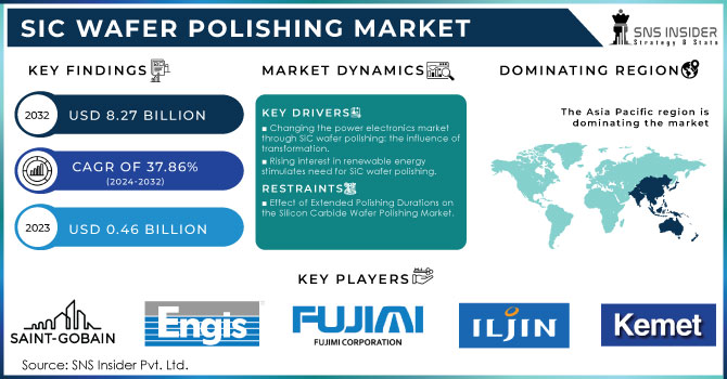
The SiC Wafer Polishing Market size was valued at USD 0.46 Billion in 2023 and is expected to grow to USD 8.27Billion by 2032 and grow at a CAGR of 37.86% over the forecast period of 2024-2032.
The demand for polishing SiC wafers is significant in the semiconductor manufacturing sector, driven by the increasing requirement for silicon carbide (SiC) wafers in power electronics, notably in electric vehicles (EVs), renewable energy setups, and industrial applications. Silicon carbide is favored over traditional silicon due to its superior thermal conductivity, higher breakdown voltage, and ability to operate at high temperatures, important for high-performance power devices. The polishing of SiC wafers is essential for creating flawless, top-quality wafers. This procedure consists of chemical-mechanical polishing (CMP) to make the wafer surface smoother and eliminate imperfections, guaranteeing that the SiC devices adhere to strict performance criteria. The need for high-quality CMP tools and consumables is increasing as the demand for flawless wafers rises in order to create top-notch semiconductors. The SiC wafer polishing industry is set for strong growth due to advancements in power electronics and the increasing need for efficient, high-performing devices. Yet, issues regarding production expenses and limitations in the supply chain must be resolved in order for the market to maximize its capabilities.
The shift to electric vehicles is causing a major growth in the automotive semiconductor sector, with silicon carbide (SiC) and gallium nitride (GaN) technologies playing a vital role. As electric vehicles (EVs) evolve, advanced components are crucial for power converters to be efficient and long-lasting. By 2030, it is anticipated that over half of the semiconductor content in vehicles will be made up of discrete devices such as MOSFETs and IGBTs, leading to a rise in the average vehicle cost from USD 301 to USD 563. SiC and GaN semiconductors are gaining popularity for these uses because they can operate at higher frequencies, voltages, and temperatures compared to conventional silicon-based semiconductors. SiC is commonly utilized in EV powertrains to enhance efficiency and reduce energy loss, with GaN set to be adopted in the EV sector in the near future. The growing demand for SiC devices is closely tied to the SiC wafer polishing industry, because the effectiveness and functionality of these power electronics depend on how precisely the polishing is done. SiC wafer polishing, typically achieved with chemical-mechanical polishing (CMP), and ensures perfect, very smooth surfaces necessary for high-frequency, high-voltage automotive components to work properly. Due to the rising popularity of electric cars and the increasing significance of discrete semiconductors in vehicle design, the SiC wafer polishing market is expected to greatly expand. The provision of high-quality SiC substrates will help drive the automotive industry towards electrification by enhancing power efficiency in electric vehicles. Investing in SiC polishing technologies is essential for maintaining the supply of advanced materials, promoting creativity, and opening up new opportunities in the automotive sector.
Substantial expansion in the SiC wafer polishing industry is driven by advancements in semiconductor manufacturing technologies, particularly the emergence of Plasma Polish Dry Etch (PPDE) as a feasible alternative to the conventional Chemical Mechanical Polishing (CMP). The automotive industry is increasingly shifting to electric vehicles, making SiC wafers more critical due to their superior performance in high-power applications. According to forecasts from the industry, there will be a notable rise in the need for SiC wafers, especially within the automotive sector where there is a deficiency of 6-inch wafers. The increasing demand aligns with the rising trend oasEMIf SiC devices being used in power converters such as inverters and on-board chargers (OBCs). Oxford Instruments has introduced PPDE technology to address CMP limitations, providing a cost-effective, scalable, and environmentally friendly polishing solution. Unlike CMP, which is water-intensive and expensive to operate, PPDE offers a touchless alternative that reduces substrate stress, enhances surface quality, and lowers wafer costs. PPDE's ability to manufacture high-quality SiC substrates without any damage is crucial for minimizing defects in epitaxial growth, thus meeting the demanding standards for automotive and energy applications. The advance in technology is predicted to drive a notable expansion in the SiC wafer polishing sector by facilitating the production of top-notch SiC wafers vital for the rapidly developing electrification and sustainable energy sectors. Implementing innovative polishing methods like PPDE will be essential in order to satisfy the increasing need for SiC substrates, as the automotive sector aims to enhance efficiency and power density in electric vehicles and renewable energy systems
| Report Attributes | Details |
|---|---|
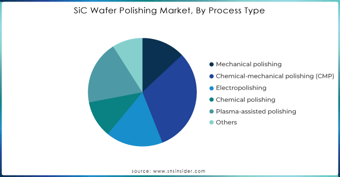
| Key Segments | • By Process Type (Mechanical polishing, Chemical-mechanical polishing (CMP), Electropolishing, Chemical polishing, Plasma-assisted polishing, Others) • By Product Type (Abrasive powders, Polishing pads, Diamond slurries, Colloidal silica suspensions, Others) • By Application (Power Electronics, Light-emitting diodes (LEDs), Sensors and detectors, Rf and microwave devices, Others) |
| Regional Coverage | North America (US, Canada, Mexico), Europe (Eastern Europe [Poland, Romania, Hungary, Turkey, Rest of Eastern Europe] Western Europe] Germany, France, UK, Italy, Spain, Netherlands, Switzerland, Austria, Rest of Western Europe]), Asia-Pacific (China, India, Japan, South Korea, Vietnam, Singapore, Australia, Rest of Asia-Pacific), Middle East & Africa (Middle East [UAE, Egypt, Saudi Arabia, Qatar, Rest of Middle East], Africa [Nigeria, South Africa, Rest of Africa], Latin America (Brazil, Argentina, Colombia, Rest of Latin America) |
| Company Profiles | Kemet International ,Entegris,Iljin Diamond, Fujimi Corporation,Saint-Gobain,JSR Corporation,Engis Corporation, Ferro Corporation, 3M, SKC, DuPont Incorporated, Fujifilm Holding America Corporation, AGC Inc.,Lapmaster Wolters,Shanghai Xinanna Electronic Technology Co., Ltd,Advanced Abrasives Corporation,Applied Materials,Kinik Company & Others |
Market Dynamics
Drivers
- Transforming the power electronics market by polishing SiC wafers has a significant influence on the industry.
The semiconductor industry is being greatly influenced by the rapid progress of silicon carbide (SiC) power semiconductors, especially in the automotive Market, where SiC devices are more commonly used for on-board charging, traction inversion, and DC-to-DC conversion in electric vehicles (EVs). SiC's outstanding characteristics, like its high voltage tolerance and capacity to function in high-temperature conditions, make it a compelling substitute for conventional silicon-based modules. The transition from silicon IGBTs to SiC MOSFETs, with increased power density and faster switching speed, is revolutionizing power electronics. SiC power modules are now at the same price level as silicon-based ones, according to Victor Veliadis, executive director and CTO of PowerAmerica. This equal pricing is spurring the formation of new supply collaborations and the establishment of more SiC fabs, signaling a significant change towards increased adoption. With the increase in demand for SiC wafers, there is a growing requirement for advanced polishing technologies to guarantee top-notch substrate surfaces as production boosts. The SiC wafer polishing market is set to gain from this movement, as the production of SiC devices necessitates extensive advancements in wafer technology, with 20% new tools and 80% modified tools being implemented. Achieving quicker turnaround times for both integrated and discrete power devices requires accurate and effective polishing procedures. As SiC wafers are now essential for high-performance automotive uses, advanced polishing methods like Plasma Polish Dry Etch (PPDE) are increasingly important. PPDE offers better surface quality, lower operational costs, and less environmental impact in comparison to traditional Chemical Mechanical Polishing (CMP). The correlation between the demand for top-notch SiC substrates and the progress in wafer polishing techniques highlights the potential growth in the SiC wafer polishing market, fueled by the increasing use of SiC power semiconductors in the automotive and other electronics industries.
- Rising interest in renewable energy stimulates need for SiC wafer polishing.
The rise in the renewable energy industry is having a big impact on the need for silicon carbide (SiC) wafers, underlining the importance of advanced wafer polishing methods. SiC devices play a crucial role in renewable energy applications because of their excellent efficiency, high thermal conductivity, and capability to withstand high voltages and temperatures. As governments around the world increase funding for renewable energy infrastructure like solar panels, wind turbines, and energy storage, the demand for advanced power electronics also rises. SiC-based power devices are becoming more popular in these applications due to their effectiveness in converting and controlling energy, consequently improving overall system performance and dependability. This increase in request leads to an increased requirement for SiC wafers, which need to be polished to a high level to guarantee the best performance and durability. Achieving smooth, defect-free surfaces on SiC wafers is crucial for the efficient operation of power electronics. With the growing renewable energy Market, substantial growth is anticipated in the SiC wafer polishing market. Plasma Polish Dry Etch (PPDE) and other advanced polishing methods are gaining importance for their higher surface quality, lower costs, and decreased environmental impact compared to Chemical Mechanical Polishing (CMP). The link between the increasing need for SiC devices in renewable energy use and the necessity for precise wafer polishing highlights the growth opportunities in the SiC wafer polishing market, propelled by the global shift towards sustainable energy technologies.
Restraints
- Effect of Extended Polishing Durations on the Silicon Carbide Wafer Polishing Market.
The SiC wafer polishing Market is greatly influenced by the lengthy polishing cycle times, leading to a significant impact on market growth and effectiveness. Silicon carbide (SiC) wafers are highly regarded for their outstanding characteristics like resistance to high temperatures, high power density, and minimal power loss, playing a key role in Markets such as power electronics, automotive, telecommunications, and aerospace. Although they offer benefits, the polishing of SiC wafers is still a crucial and lengthy step. The prolonged polishing time affects production capacity and throughput. Achieving the necessary surface quality and precision in SiC wafer polishing requires careful and detailed processing. Nevertheless, the extended duration required for polishing decreases overall production efficiency and may result in reduced production speeds. Consequently, producers encounter difficulties in expanding their operations to accommodate the increasing need for SiC wafers, especially in Markets with high demand. This lack of efficiency may result in shortages of supplies and delays in meeting customer demands, which could hinder market expansion. The issue is made worse by the necessity of expensive advanced polishing technologies and consumables, resulting in significant investments being needed. Even though Plasma Polish Dry Etch (PPDE) shows promise in surpassing Chemical Mechanical Polishing (CMP), the widespread implementation of this new method is still underway.
MARKET SEGMENTATION
By Process Type
-
Mechanical polishing
-
Chemical-mechanical polishing (CMP)
-
Electropolishing
-
Chemical polishing
-
Plasma-assisted polishing
-
Others
Get Customized Report as per your Business Requirement - Request For Customized Report
By Product Type
-
Abrasive powders
-
Polishing pads
-
Diamond slurries
-
Colloidal silica suspensions
-
Others
By Application
-
Power Electronics
-
Light-emitting diodes (LEDs)
-
Sensors and detectors
-
RF and microwave devices
-
Others
REGIONAL ANALYSIS
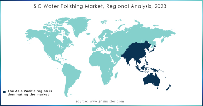
From 2023 to 2028, the Sic wafer polishing market is anticipated to grow at the highest CAGR in the Asia Pacific region. Taking into account these facts, Asia Pacific is one of the largest markets for sic wafer polishing. The region is a major hub for the electronics and semiconductor industry, with nations like China, Japan, South Korea, and Taiwan is a major producer of semiconductors worldwide. The increasing requirement for high-quality polished SiC wafers is being driven by the rising demand for SiC-based products, such as power electronics, RF components, and LEDs encouraging the market for polishing to grow. With a growing population and increasing disposable incomes fueling demand for smartphones, tablets, and other electronic gadgets, the Asia Pacific area is home to a sizable consumer electronics market. The need for polished SiC wafers is being driven further by the rising use of SiC-based power devices in contemporary consumer electronics for improved efficiency and longer battery life.
KEY PLAYERS
Some of the key Players in SiC Wafer Polishing Market with their products and offering
- Kemet International – (Kemet Kross-Linked Polishing Pads)
- Entegris – (Entegris Advanced CMP Slurries)
- Iljin Diamond – (Iljin Diamond Polishing Pads)
- Fujimi Corporation – (Fujimi CMP Slurries for SiC)
- Saint-Gobain – (Saint-Gobain Polishing Pads and Slurries)
- JSR Corporation – (JSR CMP Slurries and Polishing Pads)
- Engis Corporation – (Engis Diamond Polishing Pads and Slurries)
- Ferro Corporation – (Ferro CMP Slurries)
- 3M – (3M Polishing Pads and Slurries for SiC)
- SKC – (SKC CMP Slurries and Polishing Pads)
- DuPont Incorporated – (DuPont CMP Slurries for SiC)
- Fujifilm Holding America Corporation – (Fujifilm CMP Pads and Slurries)
- AGC Inc. – (AGC Polishing Pads and Slurries)
- Lapmaster Wolters – (Lapmaster Polishing Pads and Equipment)
- Shanghai Xinanna Electronic Technology Co., Ltd – (Xinanna Polishing Pads for SiC)
- Advanced Abrasives Corporation – (Advanced Abrasives CMP Slurries)
- Applied Materials – (Applied Materials Polishing Equipment and Slurries)
- Kinik Company – (Kinik Polishing Pads and Slurries for SiC)
- Others – (Various products depending on the specific company)
RECENT DEVELOPMENT
-
In July 2023, SKC decided to acquire ISC, a semiconductor test solution provider
-
In August 2023, Entegris, Inc., an American company specializing in polishing SiC wafers, purchased the SiC wafer polishing division of Japan's Showa Denko K.K. for $700 Billion. The acquisition grants Entegris the ability to utilize Showa Denko's knowledge in creating and producing SiC wafer polishing pads and slurries.
-
In September 2023, Lam Research Corporation, an American semiconductor equipment company, collaborated with Tokyo Electron Limited (TEL), a Japanese semiconductor equipment company, to create and market innovative SiC wafer cleaning equipment.
-
October 2023: Beijing Semiconductor Research Equipment Co., Ltd., a Chinese company specializing in semiconductor equipment. (BSRI) collaborated with Aixtron SE, a semiconductor equipment company based in Germany, to create and bring to market innovative SiC wafer epitaxy equipment.
| Report Attributes | Details |
| Market Size in 2023 | USD0.46 billion |
| Market Size by 2032 | USD 8.27 billion |
| CAGR | CAGR of 37.86 % From 2024 to 2032 |
| Base Year | 2023 |
| Forecast Period | 2024-2032 |
| Historical Data | 2020-2022 |
| Report Scope & Coverage | Market Size, Segments Analysis, Competitive Landscape, Regional Analysis, DROC & SWOT Analysis, Forecast Outlook |
| Key Drivers |
• Transforming the power electronics market by polishing SiC wafers has a significant influence on the industry. • Rising interest in renewable energy stimulates need for SiC wafer polishing.
|
| Market Restrain |
• Effect of Extended Polishing Durations on the Silicon Carbide Wafer Polishing Market
|
Get in Touch
