Wafer Cleaning Equipment Market Report Scope and Overview:
The Wafer Cleaning Equipment Market size was USD 10.23 Billion in 2025E and expected reach USD 15.61 billion till the end of year 2033 with CAGR of 5.43% over the forecast period 2026-2033.
The growing demand for electronics is driving the expansion of the wafer cleaning equipment market, as consumers and industries increasingly require high-performance, defect-free chips. Wafer cleaning systems are crucial for ensuring these chips meet strict quality and functionality standards. The rise of smart devices, 5G networks, and printed electronics further emphasizes the need for advanced cleaning technologies. Wafers are also vital in optoelectronics, powering devices like photodiodes and laser diodes. Government initiatives, such as the US CHIPS and Science Act, support wafer production facilities and equipment adoption, boosting market growth. Additionally, the medical sector relies on clean, reliable semiconductors for high-tech clinical devices, while academic and research institutions depend on wafer cleaning systems for preparing contamination-free substrates in experimental and R&D applications.
Wafer Cleaning Equipment Market Size and Forecast:
-
Market Size in 2025E: USD 10.23 Billion
-
Market Size by 2033: USD 15.61 Billion
-
CAGR: 5.43% from 2026 to 2033
-
Base Year: 2025E
-
Forecast Period: 2026–2033
-
Historical Data: 2022–2024

Get More Information on Wafer Cleaning Equipment Market - Request Sample Report
Wafer Cleaning Equipment Market Highlights:
-
Increasing demand for mature node wafers is driving upgrades and proactive maintenance of existing wafer cleaning equipment, improving overall equipment effectiveness (OEE) and fab capacity without additional tools.
-
Lean manufacturing and planned maintenance practices in wafer fabs are boosting productivity, reducing costs, and enabling sustainable chip production across industries.
-
Expansion into medtech applications, such as medical devices and high-frequency implants, is creating new opportunities for wafer cleaning equipment, supported by grants and advanced cleanroom facilities.
-
Environmental regulations and handling of toxic chemicals and dust during wafer cleaning increase operational complexity and costs for semiconductor manufacturers.
-
Recruiting and retaining skilled technicians remains challenging due to rapidly evolving chip designs, advanced cleaning processes, and the need for continuous training.
-
Improved reliability and performance of wafer cleaning machines directly enhance chip quality, supporting sectors like automotive, industrial, AI, and healthcare electronics.
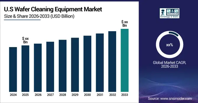
U.S. Wafer Cleaning Equipment Market Size Outlook:
The U.S. Wafer Cleaning Equipment market size was valued at an estimated USD 4.45 billion in 2025 and is projected to reach USD 6.85 billion by 2033, growing at a CAGR of 5.11% over the forecast period 2026–2033. Market growth is driven by increasing semiconductor manufacturing activities, rising demand for advanced logic and memory chips, and the growing complexity of semiconductor fabrication processes. As device geometries continue to shrink, the need for highly precise and contamination-free wafer cleaning solutions is accelerating adoption. Additionally, strong investments in domestic semiconductor fabrication facilities, advancements in wet and dry cleaning technologies, and supportive government initiatives aimed at strengthening the U.S. semiconductor supply chain further reinforce the growth outlook of the U.S. wafer cleaning equipment industry during the forecast period.
Wafer Cleaning Equipment Market Drivers:
-
Leaders in the production of computer chips are rescuing old equipment from being discarded.
The rapidly growing chip industry, driven by smartphones and AI devices, is straining production, particularly for mature node fabs (≤200 mm wafers) used in automotive, industrial, and wired communication sectors. Enhancing fab performance through proactive maintenance and optimized parts management unlocks hidden capacity in existing equipment. Cleaner wafers lead to higher-performing, more reliable chips, and studies show improved equipment reliability can boost tool availability by over 15%, increasing fab capacity by up to 10% without new tools. Applying lean manufacturing principles—streamlining inventory, reducing costs, and prioritizing planned maintenance—enables fabs to maximize efficiency, produce better chips, and sustainably meet rising global chip demand across industries.
-
Journey from Snacks to Healthcare with a Cleaning Innovation
Wafer cleaning equipment is playing a critical role in medical device manufacturing, as demonstrated by Australian chip maker Hendon Semiconductors. High-precision cleaning ensures flawless surfaces on chips used in devices like MRI machines, minimizing failures and maximizing performance. Hendon’s $605,561 seed grant is funding upgrades to cleanrooms, sterilization facilities, and wafer-to-chip-on-board processing, enabling high-frequency, reliable medical devices. By combining advanced wafer cleaning technology with new production capabilities, Hendon is accelerating medical device prototyping and manufacturing in South Australia, highlighting the crucial role of wafer cleaning in driving innovation in the medtech sector.
Wafer Cleaning Equipment Market Restraints:
-
Making wafer clean, and environment green - a Struggle for the world of integrated Circuits.
Environmental concerns pose a key restraint in the wafer cleaning equipment market. The cleaning process generates hazardous waste, toxic chemicals, and fine dust particles that can harm human health and the environment if not properly managed. Strict regulations require safe handling, storage, and disposal of these materials, as well as effective ventilation systems to capture airborne particles. Compliance increases operational complexity and costs for semiconductor manufacturers, who must invest in waste management infrastructure, secure chemical storage, and rigorous disposal procedures, making the cleaning process more resource-intensive and expensive.
Wafer Cleaning Equipment Market Segment Analysis:
By Equipment Type
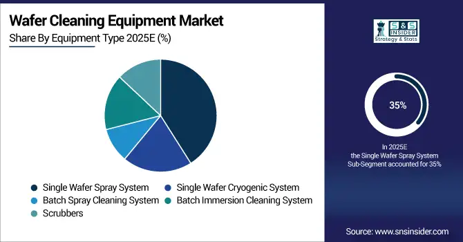
The Single Wafer Spray System dominates the wafer cleaning equipment industry with a 35% share, offering unmatched precision in cleaning delicate submicron transistors. Unlike batch systems, it sprays each wafer individually with tailored solutions, ensuring defect-free chips. Growing demand for high-performance, miniaturized semiconductors is driving market adoption.
By Application
MEMS are set to capture a 30% revenue share in the wafer cleaning equipment market by 2025. These micro-electro-mechanical systems power critical functions in smartphones, automotive sensors, and IoT devices, where even a tiny particle can cause failure. Conventional cleaning falls short, making precision wafer cleaning essential. Rising adoption of MEMS in consumer electronics and automotive applications is driving demand for advanced, highly accurate cleaning solutions.
Wafer Cleaning Equipment Market Regional Analysis:
Asia-Pacific Wafer Cleaning Equipment Market Trends:
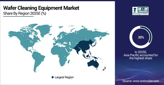
Asia Pacific is set to lead the wafer cleaning equipment market with a 30% share in 2025, driven by its concentration of advanced semiconductor fabs in China, Taiwan, South Korea, and Japan. Rapid growth in electronics, smartphones, wearables, and smart displays is boosting demand for precision cleaning solutions. Domestic investments in wafer cleaning equipment reduce reliance on foreign suppliers, while expansion in EVs and SiC power semiconductors further fuels market growth, making the region a hub for high-quality, clean chip manufacturing.
Need Customized Research Report on Wafer Cleaning Equipment Market - Enquiry Now
North America Wafer Cleaning Equipment Market Trends:
North America is projected to achieve the highest growth rate of 25% in the wafer cleaning equipment market by 2025, driven by rising investments in new semiconductor fabs, increasing demand for advanced chips enabled by AI and 5G, and government support through initiatives like the US CHIPS Act. The expansion of domestic chip manufacturing and the need for precise cleaning solutions in high-performance fabs are key drivers propelling market growth in the region.
Europe Wafer Cleaning Equipment Market Trends:
Europe is witnessing steady growth in wafer cleaning equipment, expected to reach a 15% market share by 2025. The region’s semiconductor ecosystem is anchored by countries like Germany, France, and the Netherlands, home to advanced chip fabs and packaging facilities. Europe’s growth is largely driven by the adoption of Industry 4.0 practices and automation in chip manufacturing, which demands precise wafer cleaning solutions. Government initiatives such as the European Chips Act, coupled with investments in local fabs and research centers, are further strengthening domestic capabilities. The region’s focus on automotive electronics, industrial applications, and green technologies, particularly EVs and renewable energy systems, is boosting demand for high-quality semiconductor wafers and, consequently, wafer cleaning equipment.
Latin America Wafer Cleaning Equipment Market Trends:
Latin America is expected to hold a smaller yet strategic share of the wafer cleaning equipment market, around by 2025. Brazil and Mexico are the key players, with semiconductor manufacturing primarily catering to automotive electronics, consumer electronics, and industrial devices. Growth is driven by government incentives for tech manufacturing, rising electronics consumption, and partnerships with global semiconductor players. While the market is still nascent, localized assembly and packaging units are gradually increasing the demand for precise wafer cleaning solutions to meet quality standards.
Middle East & Africa (MEA) Wafer Cleaning Equipment Market Trends:
The MEA wafer cleaning equipment industry is emerging, projected to grow at around by 2025. This growth is driven by increasing industrialization, government-backed technology parks, and investment in semiconductor infrastructure. Countries like Israel and the UAE are leading in innovation hubs and fab expansions, focusing on defense electronics, IoT, and AI applications. While the region is still developing its semiconductor manufacturing base, reliance on imported wafer cleaning tools is gradually decreasing as local partnerships and in-country production initiatives gain momentum.
Wafer Cleaning Equipment Market Competitive Landscape:
SCREEN Holdings Co., Ltd. Established in 1943, is a leading semiconductor equipment manufacturer specializing in wafer cleaning, spin scrubbers, and process solutions. The company offers high-performance, reliable, and environmentally friendly systems for advanced semiconductor production, including power devices and MEMS, serving global customers across multiple technology segments.
- In November 2024, SCREEN Semiconductor Solutions launched the SS-3200 for 200mm wafers, offering high-throughput spin scrubber cleaning optimized for power devices. The system reduces DI water usage and supports environmentally friendly wafer processing.
Entegris, Inc. Established in 1997is a global leader in materials integrity and contamination control solutions for the semiconductor and advanced manufacturing industries. The company provides filtration, wafer handling, and surface-prep technologies, including CMP and wafer cleaning solutions, enabling high-yield, reliable, and environmentally sustainable semiconductor production worldwide.
- In Aug 2024, Entegris signed a long‑term supply agreement with onsemi to provide co‑optimized CMP (Chemical Mechanical Planarization) solutions for SiC wafers, supporting onsemi’s silicon‑carbide power‑device manufacturing.
Wafer Cleaning Equipment Companies are:
-
SCREEN Holdings Co., Ltd.
-
Lam Research Corporation
-
Applied Materials Inc
-
Shibaura Mechatronics Corporation
-
Akrion Technologies
-
PVA TePLA AG
-
Entegris
-
ULTRON SYSTEMS, INC.
-
Veeco Instruments Inc.
-
SEMES
-
AXUS Technology
-
Beijing TSD Semiconductor Equipment Co., Ltd.
-
Toho Kasei Co., Ltd.
-
Cleaning Technologies Group
-
SEMETEK
-
AP&S International GmbH
-
ITW
-
RENA Technologies GmbH
| Report Attributes | Details |
|---|---|
| Market Size in 2025E | USD 10.23 Billion |
| Market Size by 2033 | USD 15.61 Billion |
| CAGR | CAGR of 5.43% From 2026 to 2033 |
| Base Year | 2025E |
| Forecast Period | 2026-2033 |
| Historical Data | 2022-2024 |
| Report Scope & Coverage | Market Size, Segments Analysis, Competitive Landscape, Regional Analysis, DROC & SWOT Analysis, Forecast Outlook |
| Key Segments |
|
| Regional Analysis/Coverage | North America (US, Canada), Europe (Germany, UK, France, Italy, Spain, Russia, Poland, Rest of Europe), Asia Pacific (China, India, Japan, South Korea, Australia, ASEAN Countries, Rest of Asia Pacific), Middle East & Africa (UAE, Saudi Arabia, Qatar, South Africa, Rest of Middle East & Africa), Latin America (Brazil, Argentina, Mexico, Colombia, Rest of Latin America). |
| Company Profiles | SCREEN Holdings Co., Ltd.; Tokyo Electron Limited; Lam Research Corporation; Applied Materials Inc.; Shibaura Mechatronics Corporation; Akrion Technologies; Modutek.com; PVA TePLA AG; Entegris; ULTRON SYSTEMS, INC.; Veeco Instruments Inc.; SEMES; AXUS Technology; Beijing TSD Semiconductor Equipment Co., Ltd.; Toho Kasei Co., Ltd.; Cleaning Technologies Group; SEMETEK; AP&S International GmbH; ITW; RENA Technologies GmbH. |
Get in Touch
