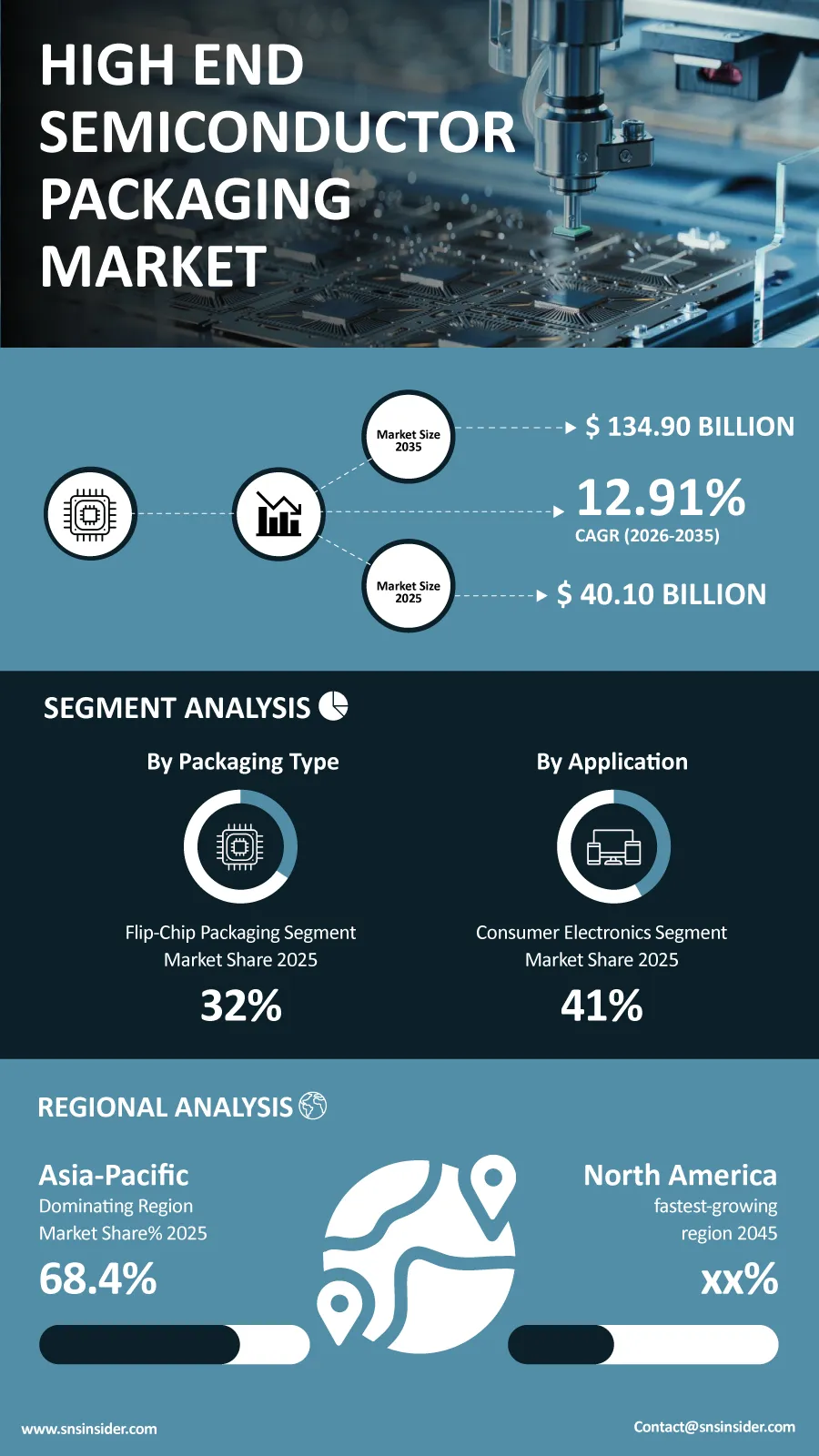
The global High End Semiconductor Packaging Market is poised for significant expansion over the coming decade due to increasing investment in advanced semiconductor packaging technology by the manufacturers to meet future performance requirements of computing systems. According to a recent study by SNS Insider, the global High End Semiconductor Packaging Market size valued at USD 40.10 billion in 2025, is anticipated to grow to USD 134.90 billion by 2035, registering a CAGR of 12.91% over the 2026–2035 forecast period.
The fast pace of development in areas such as artificial intelligence, high performance computing, 5G communications, and advanced consumer electronics is revolutionizing the design of semiconductors, making it more important than ever before to have packaging solutions that can offer better performance and power efficiency. With the advancement of chip designs, packaging solutions have started playing an integral role.
There are increased investments being made by manufacturers in innovation involving advanced packaging, chiplet technology, heterogenous integration, and three-dimensional integration of chips in order to boost computing efficiency and reduce the use of space and power. Technology is helping manufacturers in overcoming scaling challenges for complex integrated circuits.
To Get Detailed Insights on the High End Semiconductor Packaging Market – Request a Sample Report
Advanced Chip Architectures Continue to Drive Market Expansion
Rising requirements of AI accelerators, cloud computing hardware, and high-speed networking components have prompted semiconductor firms to leverage advanced packaging techniques that enhance chip density and bandwidth and hence performance. There has been the rise of packaging as an important part of innovation within the semiconductor industry since there is the need for improved functionality beyond just transistor shrinkage.
The efforts being undertaken by governments through incentives to boost the manufacturing of semiconductors in their countries have been contributing to growth in the market. This includes increased investments in foundries, OSATs, and advanced packaging infrastructure.
Moreover, advancements in fan-out wafer level packaging, systems in package, and 2.5D/3D integration technologies have led to increased applications in automotive electronics, telecommunications, industrial automation, and data centers.
Key Market Insights Highlight Shifting Demand Patterns
By packaging type, flip-chip packaging is estimated to generate 32% of total market revenue in 2025 due to its electrical performance, input/output density, and heat dissipation. The fastest-growing packaging type is projected to be 3D packaging due to increasing demand for AI processors, HPCs, and data centers in the years to come.
Based on material, the organic substrates will be responsible for 39% of total market revenue in 2025 due to their electrical connectivity, reliable structure, and suitability for complex semiconductor packages. Among materials, die attach is estimated to be the fastest-growing due to improving thermal conductivity and package reliability.
In terms of application, Consumer electronics is expected to lead the market with 41% of the revenue generated in 2025, driven by increasing demand for smartphones, tablets, wearable electronics, and premium consumer technologies. On the other hand, automotive electronics is expected to become the fastest-growing application as semiconductor solutions for electric vehicles, ADASs, and autonomous cars become necessary.
By end user, Outsourced Semiconductor Assembly and Test companies are estimated to have 55% of total market revenue in 2025 due to their advanced packaging and testing knowledge. On the other hand, foundries are expected to be the fastest-growing end users until 2035 due to direct integration of advanced packaging with wafer production.
Packaging Innovation Reshapes Next-Generation Semiconductor Design
With the ever-increasing demands placed on semiconductor technology, companies are implementing packaging technologies that will enable high levels of integration, superior signal integrity, and better power efficiency. Through chiplet technology and heterogenous integration, more than one specialized die is capable of being used as a single computational platform.
There are also advances being made in thermal management materials, substrate technologies, and manufacturing techniques which enhance the reliability of chips in tough environments like artificial intelligence, automotive electronics, telecommunication equipment, and cloud infrastructure.
It is anticipated that these developments will become increasingly significant as semiconductor manufacturers develop products for handling growing computational requirements.
Asia Pacific to Secure 68.4% Revenue Share in 2025 as North America Accelerates Semiconductor Investments
It is predicted that Asia Pacific will contribute to 68.4% of the total market revenue by 2025, but it is also anticipated to record the highest growth rate with a CAGR of 13.77% up to 2035. Asia Pacific region still enjoys the advantage of an extensive and highly developed semiconductor manufacturing value chain in Taiwan, South Korea, China, and Japan.
North America continues to be one of the key markets for growth due to increasing needs for high-performance computers, artificial intelligence, innovative network technology, and governmental programs for semiconductor fabrication on the country’s soil. The investments in advanced packaging capabilities and future chips are giving the continent competitive edge in the semiconductor industry.
Industry Participants Focus on Advanced Packaging Innovation
Competition across the High End Semiconductor Packaging Market continues to intensify as leading semiconductor companies expand production capacity while investing in advanced packaging technologies capable of supporting increasingly sophisticated chip architectures. Manufacturers are prioritizing innovations in 3D integration, system-in-package solutions, chiplet technologies, and wafer-level packaging to meet evolving customer requirements.
Key companies operating in the global High End Semiconductor Packaging Market include ASE Technology Holding Co., Ltd., Amkor Technology, Taiwan Semiconductor Manufacturing Company (TSMC), Intel Corporation, JCET Group Co., Ltd., Siliconware Precision Industries Co., Ltd. (SPIL), Powertech Technology Inc. (PTI), Tongfu Microelectronics Co., Ltd., Samsung Electronics Co., Ltd., SK Hynix Inc., Texas Instruments Incorporated, STMicroelectronics N.V., Infineon Technologies AG, UTAC Holdings Ltd., ChipMOS Technologies Inc., Hana Micron Inc., Nepes Corporation, Unisem Group, Signetics Corporation, and Advanced Micro Devices, Inc. (AMD).
An SNS Insider analyst Sushant Kadam commented, “The rapid adoption of artificial intelligence, advanced computing platforms, and heterogeneous chip architectures is fundamentally reshaping semiconductor packaging technologies. Companies investing in advanced integration capabilities, innovative materials, and high-performance packaging platforms will be well positioned to capitalize on the next phase of semiconductor industry growth.”
About the Author

Get in touch