Cloud Electronic Design Automation Market Report Scope & Overview:
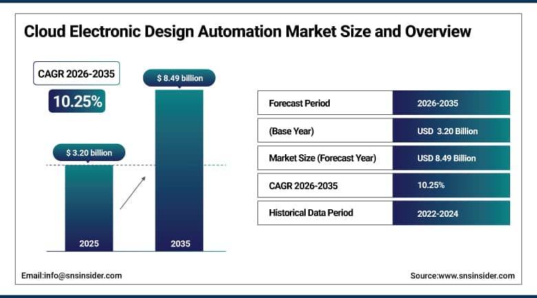
The Cloud Electronic Design Automation Market size was valued at USD 3.20 billion in 2025 and is expected to reach USD 8.49 billion by 2035, growing at a CAGR of 10.25% during 2026-2035.
Cloud electronic design automation market growth is driven by the high demand for scalable, cost-effective, and collaborative design tools across the semiconductor and electronics industries. As chips become more complex, and customers can build global teams of engineers, the importance of real-time collaboration, time-to-market, and the ability to work from anywhere increases. The market is expected to witness growth due to the use of AI/ML for design optimization, increasing adoption of IoT and automotive electronics, and moving toward fabless semiconductor business models. More enterprises that used to consider on-premises deployment choose to deploy the cloud as the infrastructure cost is lower and it is more flexible. An increase in data centers and 5G investments is increasing the need for advanced chip designs and helping EDA adoption.
Cloud Electronic Design Automation Market Size and Forecast:
-
Market Size in 2025: USD 3.20 Billion
-
Market Size by 2035: USD 8.49 Billion
-
CAGR: 10.25% from 2026 to 2035
-
Base Year: 2025
-
Forecast Period: 2026–2035
-
Historical Data: 2022–2024
To Get More Information On Cloud Electronic Design Automation Market - Request Free Sample Report
Cloud Electronic Design Automation Market Trends:
-
Rising demand for scalable, cost-effective, and collaborative cloud-based chip design tools
-
Increasing chip complexity driving adoption of advanced AI/ML-powered EDA solutions
-
Growing shift from on-premise to hybrid and public cloud deployment models
-
Expanding semiconductor applications in AI, 5G, IoT, and automotive electronics
-
Accelerating adoption of fabless semiconductor business models
-
Increasing investments in data centers and high-performance computing infrastructure
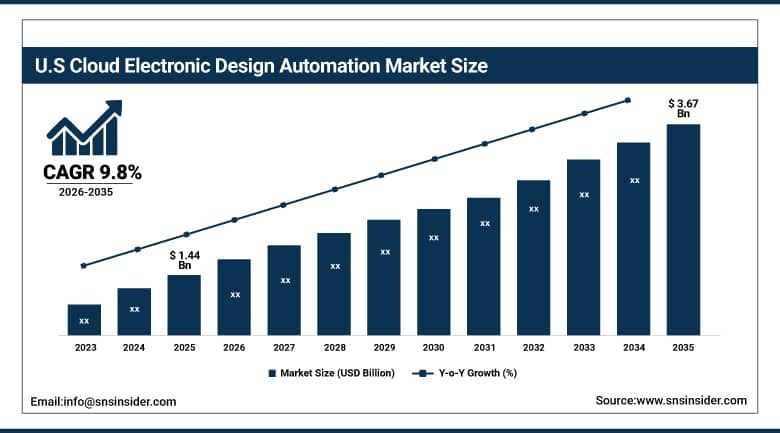
The U.S. Cloud Electronic Design Automation Market size is projected to grow from USD 1.44 Billion in 2025 to reach USD 3.67 Billion by 2035, growing at a CAGR of 9.8%.
Growth factors are increasing complexity of semiconductor design, strong domestic footprint of leading EDA companies, increasing adoption of cloud-based chip design tools, growing use of AI and HPC applications, increasing demand for advanced process nodes, and continuous R&D efforts within the US semiconductor industry.
Cloud Electronic Design Automation Market Drivers:
-
Increasing Chip Complexity Drives Demand for Advanced EDA Tools
The challenges posed by ever-shrinking semiconductor nodes and increasingly complex chip architectures have created an explosion in electronic system complexity. Smartphones, self-driving cars, and other AI-driven devices require extreme SoC (System-on-Chip) integration and multilayer PCBs. Such evolution creates a demand for superior EDA tools that can deal with high transistor density, heterogeneous integration, and multi-domain verification. This trend is further accelerated by cloud-based EDA tools that allow faster simulation and real-time collaboration. As the time-to-market expectation is ever shorter and the requirement for first-time-right silicon is increasing, it is imperative to have intelligent automation over the design platforms, which makes EDA software not just indispensable in the chip design life-cycle but also a critical growth enabler in the electronics ecosystem.
Cloud Electronic Design Automation Market Restraints:
-
High Licensing and Ownership Costs Limit Adoption Among SMEs
Although the need to adopt EDA tools is becoming ever so important, they are expensive, particularly to startups and small-scale design centers. The cost is mainly in terms of subscription or user license, which comes with a huge investment cost. Additionally, most EDA tools require hardware, which in turn requires skilled manpower, making the cost even higher. However, with cloud EDA, hardware is not a problem, but it comes with a cost in terms of subscription, which is a huge expense to most users. The cost is a barrier to the scalability of EDA in emerging economies, thus becoming a problem to the growth of EDA. Moreover, with the complexity in software packages, the cost of training inputs in software systems is a problem to most users, which may eventually affect the widespread use and acceptance of EDA by industry.
In 2023, approximately 41% of small and mid-sized design houses reported that prohibitive licensing fees were a major reason for not adopting advanced EDA solutions.
Cloud Electronic Design Automation Market Opportunities:
-
Growth of AI, 5G, and Automotive Electronics Expands EDA Application Scope
The deployment of 5G networks globally, improved artificial intelligence, and the explosion of EVs and self-driving cars are opening a wide range of potential for the EDA market. They need more customization and high-performance chips, which will require specialized EDA solutions for RF design, AI accelerators, and power-efficient architectures. For these next-gen apps, with Cloud EDA, fast design cycles are possible, along with high scalability and access to AI-based simulation and verification tools. With a growing need for intelligent and connected systems across industries, the market will also see increased demand for application-specific integrated circuits (ASICs) and high-performance (HP) and embedded system-on-chip (SoC), presenting a profitable context for EDA vendors to expand their portfolio and territory.
Cloud Electronic Design Automation Market Challenges:
-
Security Risks in Cloud Platforms Slow Cloud EDA Adoption
Although EDA tools based in the cloud promise more scalability and opportunities for co-design, they also create major issues around data security and IP (intellectual property) protection. Since chip design requires highly sensitive data, moving workloads to the cloud will increase their susceptibility to cyber threats, data breaches, and unauthorized access. This leads to bordering regulatory compliance issues as well (cross-border data storage). Many companies, though, are still reluctant to make the leap from on-premises EDA platforms to the cloud, despite encryption and access control measures, as a fear of IP theft or leakage.
Cloud Electronic Design Automation Market Segment Analysis:
-
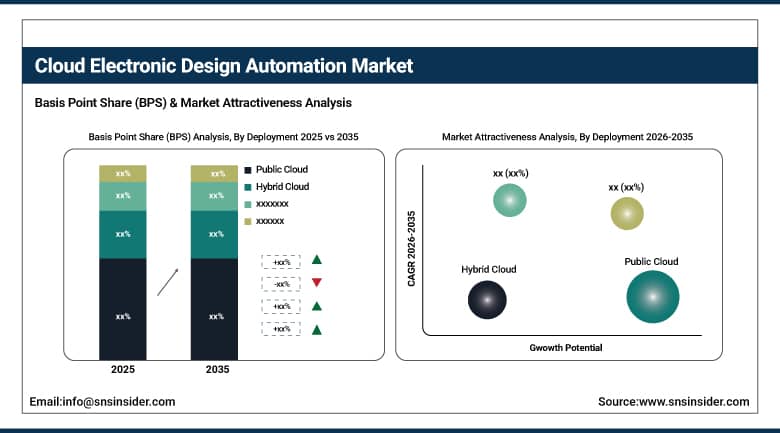
By Deployment: In 2025, Public Cloud dominated with 45% share; Hybrid Cloud fastest growing segment during 2026–2035.
-
By Product Type: In 2025, IC Physical Design & Verification dominated with 38% share; Semiconductor Intellectual Property fastest growing segment during 2026–2035.
-
By Enterprise Size: In 2025, Large Enterprises dominated with 60% share; Small & Medium Enterprises (SMEs) fastest growing segment during 2026–2035.
-
By End-User Industry: In 2025, Automotive dominated with 30% share; Healthcare fastest growing segment during 2026–2035.
By Deployment: Public Cloud Dominate, Hybrid Cloud Fastest-Growing
Public Cloud dominates the deployment segment. Its leadership is attributed to scalability, cost efficiency, and ease of access for startups and SMEs that cannot afford on-premise high-performance computing infrastructure. Public cloud EDA solutions enable companies to rent computing power as needed, avoiding heavy upfront investments in servers and storage, which is particularly advantageous for projects with fluctuating computational demands.
Hybrid Cloud is the fastest-growing deployment segment because it combines the benefits of both public and private clouds. Enterprises can store sensitive IP in private clouds while leveraging public cloud resources for heavy simulation and verification workloads. This model provides flexibility, enhanced security, and collaboration capabilities, especially in global R&D teams. Increasing adoption of hybrid deployment models in regions with advanced semiconductor industries is fueling growth.
By Product Type: IC Physical Design & Verification Dominate, Semiconductor Intellectual Property Fastest-Growing
IC Physical Design & Verification holds a strong position as a product type in the industry. This is because of the increased complexity of integrated circuit (IC) designs, which has resulted in increased demand for physical design, verification, and testing tools. This has helped the industry, as large semiconductor companies have been able to leverage these tools for increased accuracy, better design, and reduced time-to-market. The advent of AI, 5G, and high-performance computing has further increased the adoption of IC physical design & verification tools in cloud environments.
Semiconductor IP holds the position of the fastest-growing product type segment, which is a result of the increased need for IP, which accelerates the design of ICs, thus reducing design costs. This has helped the industry, as IP cores provide an opportunity for designers to integrate functional components without developing them from scratch, thus accelerating the design process.
By Enterprise Size: Large Enterprises Dominate, SMEs Fastest-Growing
Large Enterprises hold a significant share in the enterprise size category. Their market leadership is based on their large IC and PCB design capabilities, high R&D investments, and existing relationships with EDA vendors. Large enterprises often have to invest in high-performance computing to cater to their complex verification needs. Hence, they would find cloud-based EDA services very attractive.
Small & Medium Enterprises are the fastest-growing segment because of the cost-effectiveness, scalability, and accessibility offered by the cloud. Cloud EDA is helping SMEs to effectively compete with Large Enterprises without requiring huge capital expenditures. The rise of start-ups in semiconductor design, IoT, and consumer electronics is another factor driving this growth because SMEs can leverage the cloud to quickly prototype and verify their designs.
By End-User Industry: Automotive Dominate, Healthcare Fastest-Growing
Automotive is the largest end-user in the industry segment. The adoption rate of advanced driver-assistance system (ADAS), electric vehicle (EV), and infotainment technologies has fueled the demand for cloud-based EDA solutions. Automotive manufacturers use IC and PCB designs in safety-critical applications. The cloud facilitates faster design cycles and global collaboration.
The healthcare industry is the fastest-growing end user, driven by the increasing use of wearables, diagnostic tools, and image processing systems that are all moving towards the use of custom ICs and PCBs. Cloud-based EDA tools help healthcare device makers accelerate simulation, verification, and optimization of their designs while minimizing time to market. The trend towards telemedicine, portable health monitors, and smart medical devices is another driver of cloud-based EDA adoption.
Cloud Electronic Design Automation Market Regional Analysis:
North America Cloud Electronic Design Automation Market Insights:
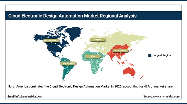
North America was at the forefront in the Cloud EDA market in 2025, with a share of 42%. This is because the region has significant semiconductor companies, strong cloud computing infrastructure, and high adoption rates for cloud-based design tools. This is also because the region has high demand for ICs, SoCs, and automotive electronics. Additionally, the region has strong R&D investments in the U.S. and Canada. This is also because the region has collaborations between chip designers and cloud-based EDA companies.
Get Customized Report as Per Your Business Requirement - Enquiry Now
Europe Cloud Electronic Design Automation Market Insights:
Europe is a key region in the global Cloud EDA industry, with high penetration in the automotive, aerospace, and industrial electronics markets. The region is keen on R&D, smart manufacturing, and adherence to extremely high regulatory standards, thus driving the adoption of cloud EDA. The region is boosted by partnerships between semiconductor firms and cloud vendors, which accelerate design, foster collaboration, and deliver cost-effective access to powerful computing resources on the continent.
Asia-Pacific Cloud Electronic Design Automation Market Insights:
Asia-Pacific is the fastest-growing cloud EDA market, which is expected to grow at a CAGR of 12.5% from 2026 to 2035. The region is benefiting from the rapid expansion of semiconductor manufacturing facilities in China, Taiwan, Japan, and South Korea; growing demand for ICs, SoCs, and auto electronics; and the growing adoption of cloud-based design and verification software. Investments in R&D, government support to chip manufacturing, and the growing base of SMEs driving cloud EDA adoption are contributing to the rapid growth of the Asia-Pacific region.
Latin America Cloud Electronic Design Automation Market Insights:
Latin America is an emerging cloud EDA market, with growth being fueled by the increasing adoption of cloud computing solutions by SMEs and electronics companies. Latin America is gradually investing in semiconductor design, automotive electronics, and industrial automation, which is encouraging the use of cloud EDA. The cloud EDA allows companies to transcend infrastructure limitations, saving costs while benefiting from advanced design and verification capabilities, which is driving the electronics and semiconductor industry in Latin America towards digital transformation and innovation.
Middle East & Africa (MEA) Cloud Electronic Design Automation Market Insights:
The MEA region is an emerging market for Cloud EDA due to increasing investments in industrial automation, electronics, and smart infrastructure projects. The usage of Cloud EDA in this region is growing gradually as organizations are utilizing cloud-based design and verification tools to overcome infrastructure challenges and minimize operational expenditures. Cloud EDA facilitates innovation in semiconductor and electronics design in key countries in MEA by providing remote collaboration and access to high-end computing resources.
Cloud Electronic Design Automation Market Competitive Landscape:
Synopsys, Inc. was founded in 1986 and is a global leader in electronic design automation (EDA) and semiconductor IP, headquartered in the USA. Synopsys provides software, IP, and services that help engineers design and verify complex integrated circuits (ICs), system-on-chips (SoCs), and electronic systems. Its solutions include IC design and verification tools, prototyping, and simulation platforms that accelerate chip development for industries such as automotive, aerospace, consumer electronics, and telecommunications. Synopsys has a presence in over 25 countries and employs more than 20,000 people worldwide.
-
In June 2025, Synopsys received Frost & Sullivan’s 2025 Global Technology Innovation Leadership Award for its AI-powered analog-in-memory computing EDA suite, reinforcing its cloud leadership.
Cadence Design Systems, Inc. was founded in 1988 and is a leading global provider of electronic design automation (EDA) solutions, headquartered in the USA. Cadence offers software, hardware, and IP that assist engineers in designing, verifying, and optimizing complex ICs, printed circuit boards (PCBs), and SoCs. Its solutions serve industries including automotive, aerospace, telecommunications, healthcare, and consumer electronics. Cadence operates in more than 25 countries and employs over 12,000 professionals worldwide.
-
In February 2024, Cadence Design Systems introduced the Millennium M1 Multiphysics Platform, enhancing CFD-based digital twin capabilities for large-scale cloud simulation.
Cloud Electronic Design Automation Market Key Players:
-
Synopsys, Inc.
-
Siemens EDA (Mentor Graphics)
-
ANSYS, Inc.
-
Keysight Technologies, Inc.
-
Altium Limited, Zuken Inc.
-
Altair Engineering, Inc.
-
Silvaco, Inc.
-
Arm Holdings
-
Broadcom Limited
-
Xilinx (AMD)
-
Agnisys
-
Aldec
-
Xpeedic
-
JEDA Technologies
-
MunEDA
-
Sigrity, Inc.
-
Alphawave Semi
-
Imperas Software Ltd.
| Report Attributes | Details |
|---|---|
| Market Size in 2025 | USD 3.20 Billion |
| Market Size by 2035 | USD 8.49 Billion |
| CAGR | CAGR of 10.25% From 2026 to 2035 |
| Base Year | 2025 |
| Forecast Period | 2026-2035 |
| Historical Data | 2022-2024 |
| Report Scope & Coverage | Market Size, Segments Analysis, Competitive Landscape, Regional Analysis, DROC & SWOT Analysis, Forecast Outlook |
| Key Segments | • By Product Type: (Computer Aided Engineering, Semiconductor Intellectual Property, IC Physical Design & Verification, Printed Circuit Board & Multi-Chip Module) • By Deployment: (Public Cloud, Private Cloud, Hybrid Cloud) • By Enterprise Size: (Large Enterprises, Small & Medium Enterprises (SMEs)) • By End-User Industry: (Automotive, Aerospace & Defense, Industrial, Healthcare, Telecommunication, Others) |
| Regional Analysis/Coverage | North America (US, Canada), Europe (Germany, UK, France, Italy, Spain, Russia, Poland, Rest of Europe), Asia Pacific (China, India, Japan, South Korea, Australia, ASEAN Countries, Rest of Asia Pacific), Middle East & Africa (UAE, Saudi Arabia, Qatar, South Africa, Rest of Middle East & Africa), Latin America (Brazil, Argentina, Mexico, Colombia, Rest of Latin America). |
| Company Profiles | Synopsys, Inc., Cadence Design Systems, Inc., Siemens EDA (Mentor Graphics), ANSYS, Inc., Keysight Technologies, Inc., Altium Limited, Zuken Inc., Altair Engineering, Inc., Silvaco, Inc., Arm Holdings, Broadcom Limited, GlobalFoundries, Inc., Xilinx (AMD), Agnisys, Aldec, Xpeedic, JEDA Technologies, MunEDA, Sigrity, Inc., Alphawave Semi, Imperas Software Ltd. |
Frequently Asked Questions
Ans: The Cloud Electronic Design Automation Market is expected to grow at a CAGR of 10.25% during 2026–2035.
Ans: The Cloud Electronic Design Automation Market was valued at USD 3.20 Billion in 2025 and is expected to reach USD 8.49 Billion by 2035.
Ans: Key drivers include increasing chip complexity, rising demand for scalable and collaborative cloud-based design tools, growing adoption of AI/ML for design optimization, expansion of 5G, IoT, and automotive electronics, and the shift toward fabless semiconductor business models.
Ans: The Public Cloud segment dominated the Cloud Electronic Design Automation Market in 2025, accounting for 45% of the market share.
Ans: North America dominated the Cloud Electronic Design Automation Market in 2025, accounting for 42% of revenue share.
Get in Touch
