Die-to-Die IP Market Report Scope & Overview:
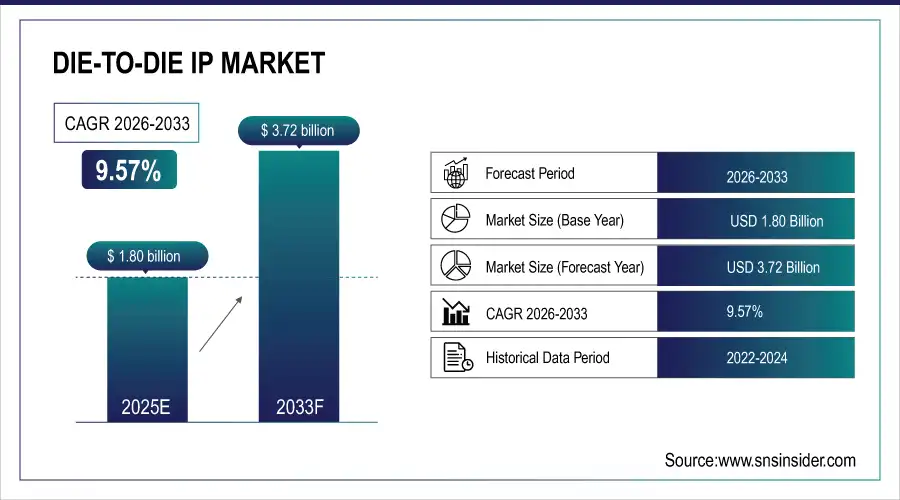
The Die-to-Die IP Market size was valued at USD 1.80 Billion in 2025E and is projected to reach USD 3.72 Billion by 2033, growing at a CAGR of 9.57% during 2026-2033.
The Die-to-Die IP market is growing due to the rapid adoption of chiplet-based architectures that enable higher performance, lower power consumption, and reduced design costs compared to monolithic chips. Increasing demand for AI accelerators, high-performance computing, and data-center processors is driving the need for high-bandwidth, low-latency interconnects. Advancements in 2.5D and 3D packaging, rising UCIe standard adoption, and growing semiconductor complexity further support market expansion across automotive, consumer, and industrial applications.
Market Size and Growth Projection:
-
Market Size in 2025E USD 1.80 Billion
-
Market Size by 2033 USD 3.72 Billion
-
CAGR of 9.57% From 2026 to 2033
-
Base Year 2025E
-
Forecast Period 2026-2033
-
Historical Data 2021-2024
To Get more information On Die-to-Die IP Market - Request Free Sample Report
Key Die-to-Die IP Market Trends
-
Rapid adoption of chiplet-based architectures replacing traditional monolithic SoC designs for higher performance and efficiency.
-
Growing demand from HPC, AI, machine learning, and data center processors requiring high-bandwidth, low-latency die-to-die interconnects.
-
Advancements in 2.5D and 3D IC packaging and increasing use of open standards like UCIe for interoperability.
-
Expansion of the chiplet ecosystem into automotive, ADAS, and autonomous driving applications with safety-critical performance needs.
-
Increasing investments in Asia Pacific semiconductor manufacturing, advanced packaging, and custom silicon development by hyperscalers and system OEMs.
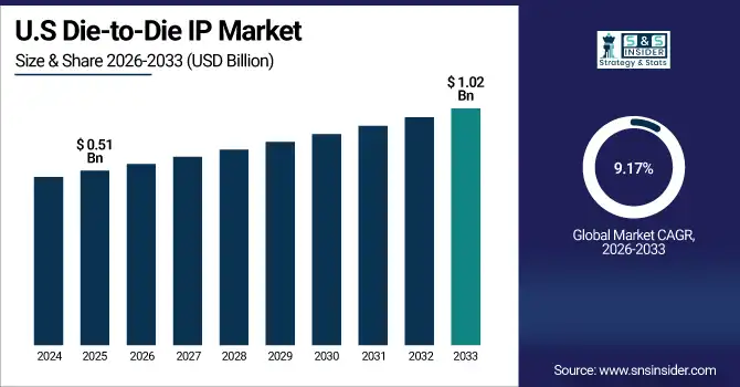
The U.S. Die-to-Die IP Market size was valued at USD 0.51 Billion in 2025E and is projected to reach USD 1.02 Billion by 2033, growing at a CAGR of 9.17% during 2026-2033. The U.S. Die-to-Die IP market is growing due to strong investments in AI and high-performance computing, rapid adoption of chiplet architectures by leading semiconductor companies, advanced packaging leadership, and increased demand from hyperscalers for high-bandwidth, energy-efficient interconnect solutions.
Die-to-Die IP Market Growth Drivers:
-
Rapid Shift to Chiplet Architectures Drives Global Die-to-Die IP Market Growth Across HPC AI and Advanced Packaging
The global Die-to-Die IP market is primarily driven by the rapid transition from monolithic system-on-chip designs to chiplet-based architectures, which enable higher performance, improved yield, and lower development costs. Rising demand for high-performance computing, artificial intelligence, machine learning, and data center processors requires ultra-high bandwidth, low-latency, and energy-efficient interconnect solutions between multiple dies. Advancements in advanced packaging technologies such as 2.5D and 3D IC integration, along with growing adoption of open standards like UCIe, are accelerating interoperability and ecosystem maturity. Additionally, increasing semiconductor design complexity at advanced nodes and the need to optimize power and thermal efficiency are reinforcing the adoption of die-to-die interconnect IP across automotive, networking, and consumer electronics applications.
Chiplet-based designs now generate about USD 40 billion in annual revenue, showing how widespread modular multi-die integration has become in high-performance electronics.
Die-to-Die IP Market Restraints:
-
Die-to-Die IP Market Constrained by Standardization Challenges Complex Designs and Thermal Management Limitations
The Die-to-Die IP market faces restraints from limited standardization beyond early UCIe adoption, creating interoperability challenges across vendors and ecosystems. Design complexity, signal integrity issues at high data rates, and thermal management constraints in advanced packaging hinder faster adoption. Additionally, lengthy qualification cycles in automotive and industrial applications, along with IP integration and validation challenges across heterogeneous dies, slow large-scale deployment.
Die-to-Die IP Market Opportunities:
-
Expanding Chiplet Ecosystem Unlocks Global Die-to-Die IP Opportunities Across Automotive AI and Emerging Markets
Significant opportunities exist as the chiplet ecosystem expands across new end-use sectors beyond HPC and data centers. Automotive electronics, including ADAS and autonomous driving platforms, present strong growth potential due to rising compute requirements and safety-critical performance needs. Emerging markets in Asia Pacific are creating opportunities through heavy investments in semiconductor manufacturing, advanced packaging, and domestic chip design initiatives. Furthermore, growing participation of hyperscalers and system OEMs in custom silicon development is opening new demand for scalable, standardized die-to-die IP solutions. Continuous innovation in 3D stacking, heterogeneous integration, and open interface standards will further unlock long-term growth opportunities globally.
The P7+ electric sedan from Xpeng uses two Nvidia Orin X processors to deliver over 500 TOPS of compute from multiple sensor inputs, showing real deployment of high-performance compute in vehicles that could benefit from modular chiplets.
Die-to-Die IP Market Segment Analysis
-
By Interface Standard, UCIe (Universal Chiplet Interconnect Express) dominated with 53.43% in 2025E, and it is expected to grow at the fastest CAGR of 9.92% from 2026 to 2033.
-
By Packaging Technology, 2.5D IC Packaging dominated with 39.97% in 2025E, and 3D IC Packaging is expected to grow at the fastest CAGR of 10.10% from 2026 to 2033.
-
By Application, High-Performance Computing (HPC) & AI Accelerators dominated with 41.86% in 2025E, and it is expected to grow at the fastest CAGR of 9.83% from 2026 to 2033.
-
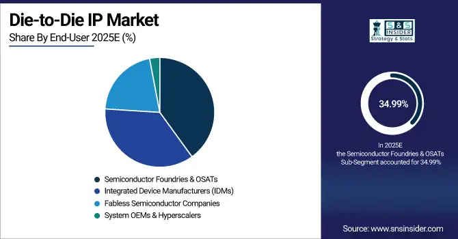
By End-User, Semiconductor Foundries & OSATs dominated with 34.99% in 2025E, Fabless Semiconductor Companies is expected to grow at the fastest CAGR of 10.12% from 2026 to 2033.
By End-User, Semiconductor Foundries Lead 2025E Die-to-Die IP Market While Fabless Firms Drive Future Growth
Semiconductor Foundries & OSATs dominate the Die-to-Die IP market in 2025E, driven by their role in advanced packaging, multi-die integration, and providing scalable solutions for multiple clients across HPC, AI, and automotive applications. Fabless Semiconductor Companies are expected to grow fastest from 2026–2033 as they increasingly adopt standardized chiplet architectures and die-to-die IP to accelerate time-to-market, enhance performance, and reduce design complexity, supported by growing collaboration with foundries, system OEMs, and hyperscalers globally.
By Interface Standard, UCIe Standard Dominates 2025E Market and Fuels Rapid Future Growth in Die-to-Die Chiplet Integration
The UCIe (Universal Chiplet Interconnect Express) standard is dominant in 2025E due to its open, interoperable architecture, enabling seamless communication between chiplets from different vendors. Its adoption across high-performance computing, AI accelerators, and data center processors drives widespread industry support. UCIe is expected to grow fastest from 2026–2033, fueled by increasing demand for modular, high-bandwidth, and energy-efficient multi-die systems, expanding chiplet ecosystems, and continuous innovation in heterogeneous integration and advanced packaging technologies.
By Packaging Technology, 2.5D IC Packaging Leads 2025E Market While 3D IC Packaging Accelerates Future Die-to-Die Growth
2.5D IC Packaging is dominant in 2025E due to its maturity, cost-effectiveness, and ability to integrate multiple dies on an interposer, offering high performance and reliable connectivity for HPC, AI, and data center applications. 3D IC Packaging is expected to grow fastest from 2026–2033, driven by increasing demand for higher interconnect density, improved power efficiency, and advanced heterogeneous integration in AI accelerators, automotive electronics, and next-generation computing systems. Continuous innovation in vertical stacking and thermal management supports this growth.
By Application, HPC and AI Accelerators Drive 2025E Die-to-Die IP Market with Rapid Future Growth
High-Performance Computing (HPC) & AI Accelerators dominate the Die-to-Die IP market in 2025E due to the surge in AI workloads, deep learning, and complex simulations requiring ultra-high bandwidth and low-latency interconnects. This application segment is also expected to grow fastest from 2026–2033, driven by expanding AI adoption, exascale computing initiatives, and increasing demand from data centers and cloud providers. Continuous innovation in chiplet architectures and die-to-die integration further accelerates deployment in HPC and AI systems.
North America Die-to-Die IP Market Insights
North America, holding 36.36% of the Die-to-Die IP market in 2025E, is the dominant region due to its strong semiconductor ecosystem, presence of leading chiplet and IP vendors, and early adoption of advanced packaging and UCIe standards. The region benefits from significant R&D investments, robust data center infrastructure, and growing AI and HPC applications. Close collaboration between fabless companies, foundries, and hyperscalers further strengthens North America’s leadership in die-to-die interconnect technology and high-performance compute solutions.

Get Customized Report as per Your Business Requirement - Enquiry Now
U.S. Die-to-Die IP Market Insights
The United States dominates the North American Die-to-Die IP market due to its concentration of leading semiconductor companies, advanced R&D facilities, early adoption of chiplet architectures, and strong presence of hyperscalers and high-performance computing infrastructure.
Europe Die-to-Die IP Market Insights
Europe, accounting for 16.97% of the Die-to-Die IP market in 2025E, maintains a moderate share driven by semiconductor innovation in Germany, France, and the Netherlands. The region focuses on automotive electronics, industrial automation, and defense applications, supported by advanced packaging research and collaborative chiplet initiatives. Strong emphasis on standardization, energy-efficient designs, and government-backed semiconductor programs strengthens Europe’s role in the global die-to-die interconnect ecosystem.
Germany Die-to-Die IP Market Insights
Germany dominates the European Die-to-Die IP market due to its strong automotive semiconductor industry, advanced research in chiplet and packaging technologies, and leadership in industrial automation, making it the primary contributor to Europe’s die-to-die interconnect ecosystem.
Asia Pacific Die-to-Die IP Market Insights
Asia Pacific is expected to register the fastest CAGR of 10.25% from 2026–2033 in the Die-to-Die IP market, driven by rapid semiconductor manufacturing expansion in China, Taiwan, South Korea, and Japan. Investments in advanced packaging, chiplet design, and domestic semiconductor initiatives fuel adoption. Growing demand for AI, HPC, consumer electronics, and automotive applications, combined with government support and increasing presence of fabless companies and foundries, positions Asia Pacific as the fastest-growing regional market globally.
China Die-to-Die IP Market Insights
China dominates the Asia Pacific Die-to-Die IP market due to its massive investments in semiconductor fabrication, advanced packaging facilities, chiplet R&D, government-backed initiatives, and growing demand from AI, HPC, automotive, and consumer electronics sectors.
Latin America (LATAM) and Middle East & Africa (MEA) Die-to-Die IP Market Insights
Latin America (LATAM) and Middle East & Africa (MEA) hold smaller shares of the Die-to-Die IP market but show growing potential. LATAM benefits from increasing adoption of automotive electronics, industrial automation, and emerging data center infrastructure, while MEA focuses on defense, energy, and telecommunication applications. Investments in semiconductor education, local manufacturing initiatives, and partnerships with global technology providers are gradually strengthening capabilities. Although adoption is slower than North America, Europe, and Asia Pacific, these regions offer opportunities for niche applications and strategic expansion.
Competitive Landscape for Die-to-Die IP Market:
Synopsys, Inc. is a leading global provider of electronic design automation (EDA) tools and semiconductor IP, including Die-to-Die interconnect solutions. The company offers high-performance UCIe-compliant IP, advanced PHYs, controllers, and verification platforms that enable multi-die chiplet architectures for HPC, AI, data centers, automotive, and consumer electronics. Synopsys drives innovation in heterogeneous integration and advanced packaging, helping semiconductor companies accelerate design cycles, optimize performance, and achieve reliable high-bandwidth interconnects.
-
In September 2024, Synopsys announced a 40 Gbps‑per‑pin UCIe IP suite, including controller, PHY, and verification IP to enable ultra‑high‑bandwidth die‑to‑die connectivity for multi‑die AI data center chips. The solution offers enhanced signal integrity monitoring and broad interconnect support.
Cadence Design Systems, Inc. is a leading provider of electronic design automation (EDA) tools and semiconductor IP, specializing in Die-to-Die interconnect and chiplet solutions. The company offers UCIe-compliant IP, high-speed PHYs, controllers, and verification platforms that support multi-die architectures for HPC, AI, data centers, automotive, and connectivity applications. Cadence enables faster time-to-market, high-performance integration, and scalable heterogeneous designs, driving adoption of advanced packaging and next-generation semiconductor technologies globally.
-
In April 2025, Cadence announced a significant enhancement of its design IP portfolio, including UCIe 1.1 48G die‑to‑die interconnect IP and advanced interface IP optimized for Intel’s 18A and 18A‑P technologies to accelerate AI, HPC, and mobility designs.
Die-to-Die IP Companies are:
-
Synopsys
-
Arm Holdings
-
Marvell Technology
-
Alphawave Semi
-
Rambus
-
Arteris
-
VeriSilicon
-
OpenFive
-
OPENEDGES Technology
-
Siemens EDA
-
Texas Instruments
-
NXP Semiconductors
-
Infineon Technologies
-
STMicroelectronics
-
Renesas Electronics
-
Microchip Technology
-
Analog Devices
-
ON Semiconductor
| Report Attributes | Details |
|---|---|
| Market Size in 2025E | USD 1.80 Billion |
| Market Size by 2033 | USD 3.72 Billion |
| CAGR | CAGR of 9.57% From 2026 to 2033 |
| Base Year | 2025E |
| Forecast Period | 2026-2033 |
| Historical Data | 2021-2024 |
| Report Scope & Coverage | Market Size, Segments Analysis, Competitive Landscape, Regional Analysis, DROC & SWOT Analysis, Forecast Outlook |
| Key Segments | • By Interface Standard (UCIe (Universal Chiplet Interconnect Express), BoW (Bunch of Wires), Proprietary / Custom Interfaces, and Emerging Open Standards) • By Packaging Technology (2.5D IC Packaging, 3D IC Packaging, Fan-Out Wafer-Level Packaging (FOWLP), and System-in-Package (SiP)) • By Application (High-Performance Computing (HPC) & AI Accelerators, Data Centers & Cloud Infrastructure, Consumer Electronics, and Automotive Electronics) • By End-User (Semiconductor Foundries & OSATs, Integrated Device Manufacturers (IDMs), Fabless Semiconductor Companies, and System OEMs & Hyperscalers) |
| Regional Analysis/Coverage | North America (US, Canada), Europe (Germany, UK, France, Italy, Spain, Russia, Poland, Rest of Europe), Asia Pacific (China, India, Japan, South Korea, Australia, ASEAN Countries, Rest of Asia Pacific), Middle East & Africa (UAE, Saudi Arabia, Qatar, South Africa, Rest of Middle East & Africa), Latin America (Brazil, Argentina, Mexico, Colombia, Rest of Latin America). |
| Company Profiles | Synopsys, Cadence Design Systems, Arm Holdings, Marvell Technology, Alphawave Semi, Rambus, Arteris, Blue Cheetah Analog Design, VeriSilicon, OpenFive, OPENEDGES Technology, Siemens EDA, Texas Instruments, NXP Semiconductors, Infineon Technologies, STMicroelectronics, Renesas Electronics, Microchip Technology, Analog Devices, ON Semiconductor. |
Frequently Asked Questions
North America dominated the Die-to-Die IP Market in 2025E.
UCIe (Universal Chiplet Interconnect Express) dominated the Die-to-Die IP Market.
The Die-to-Die IP market is driven by the rising adoption of chiplet architectures, growing demand for high-performance computing and AI, and advancements in 2.5D/3D packaging with standardized interconnects like UCIe.
The Die-to-Die IP Market size was USD 1.80 Billion in 2025E and is expected to reach USD 3.72 Billion by 2033.
The Die-to-Die IP Market is expected to grow at a CAGR of 9.57% from 2026-2033.
Get in Touch
