Ion Milling System Market Size & Trends:
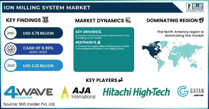
The Ion Milling System Market was valued at 2.22 Billion in 2023 and is projected to reach USD 4.78 Billion by 2032, growing at a CAGR of 8.90% from 2024 to 2032.
To Get more information on Ion Milling System Market - Request Free Sample Report
This growth is driven by the rising demand for high-precision material removal in advanced applications such as semiconductor manufacturing, nanotechnology, and research laboratories. In the United States, the market stood at USD 0.58 billion in 2023 and is expected to grow to USD 1.03 billion by 2032, with a CAGR of 6.67%. Market expansion is further supported by ongoing technological advancements, improved process efficiency, and the growing shift toward sustainable manufacturing practices. The increasing integration of AI and automation in ion milling systems is enhancing operational accuracy, reducing defects, and enabling more efficient processing. These factors collectively contribute to the rising adoption of ion milling systems across both academic and industrial environments worldwide.
Ion Milling System Market Dynamics:
Drivers:
-
Precision Surface Preparation Drives Growth in the Ion Milling System Market
The rising demand for precision surface preparation is a major driver of the Ion Milling System Market, as industries increasingly require accurate, damage-free material removal at the nanoscale. In fields such as semiconductor manufacturing, electronics, and materials science, achieving clean, artifact-free cross-sections and thin films is critical for quality control, failure analysis, and device fabrication. Ion milling systems offer unmatched precision, enabling controlled etching of complex materials without thermal damage or mechanical stress. This capability is especially valuable for preparing samples for high-resolution imaging techniques like scanning and transmission electron microscopy. As device architectures continue to shrink and materials become more complex, traditional polishing or mechanical methods fall short in delivering the required accuracy. Consequently, the growing focus on miniaturization, along with the need for reproducibility and consistency in sample preparation, is fueling the widespread adoption of ion milling systems across academic research institutions, industrial labs, and high-tech manufacturing environments.
Restraints:
-
The need for a highly skilled workforce poses a barrier to the widespread adoption of ion milling systems.
The operational complexity of ion milling systems is a significant restraint for market growth, as these systems require highly skilled personnel for setup, calibration, and operation. Unlike conventional material removal techniques, ion milling involves precise control over beam parameters, vacuum environments, and sample alignment, which demands specialized training and experience. Facilities that lack technically proficient staff may face challenges in achieving consistent and accurate results, leading to lower productivity and higher error rates. Additionally, the learning curve associated with operating advanced features such as endpoint detection or cryogenic milling can deter adoption, especially in small or resource-constrained laboratories. As a result, many organizations are hesitant to invest in ion milling systems due to the risk of underutilization or operational inefficiencies. This need for continuous training and technical expertise creates a barrier for wider implementation, particularly in regions with limited access to skilled workforce or training infrastructure.
Opportunities:
-
Growing Nanotech and Miniaturization Demands Fuel Ion Milling System Opportunities
As industries shift toward compact, high-performance electronics, there is an increasing need for precision material processing techniques that can operate at the nanoscale. Ion milling systems are uniquely suited for this, offering highly controlled etching and surface preparation without introducing thermal or mechanical damage crucial for delicate nanostructures. This demand spans sectors such as semiconductors, photonics, MEMS, and biomedical devices, where even minor defects can impact functionality. With continued miniaturization trends driven by innovations like wearable tech, IoT sensors, and next-generation computing, the role of ion milling in ensuring accurate structural analysis and quality control is becoming increasingly vital. This trend is expected to fuel adoption across research labs and advanced manufacturing facilities globally, driving market growth.
Challenges:
-
Sample sensitivity limits ion milling versatility, as delicate materials risk damage from ion beams, demanding precise process control.
Sample sensitivity remains a major challenge in the Ion Milling System Market, particularly when dealing with delicate or heat-sensitive materials. The high-energy ion bombardment used in the milling process can lead to unintended alterations such as surface amorphization, structural distortion, or even elemental loss. This is especially critical in applications involving polymers, biological specimens, or layered nanomaterials, where maintaining original morphology and composition is essential for accurate analysis. As a result, users must carefully optimize milling parameters like ion beam energy, angle of incidence, and duration to minimize damage. This sensitivity limits the system’s versatility, making it less applicable to certain advanced research or manufacturing scenarios, and driving demand for alternative techniques or hybrid systems that offer gentler processing capabilities.
Ion Milling System Market Segment Analysis:
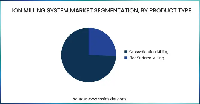
By Product Type
In 2023, the Flat Surface Milling segment dominated the ion milling system market with approximately 75% revenue share, driven by its widespread use in semiconductor manufacturing, materials science, and precision surface analysis. Its ability to deliver uniform, smooth finishes across various materials particularly metals and ceramics makes it highly favored in both industrial and research applications. The technique ensures minimal damage and high surface quality, essential for applications requiring microscopic or nanoscale evaluation. Its compatibility with a broad range of sample types and high throughput efficiency has made it the preferred choice over more specialized milling methods, contributing to its substantial market leadership. As demand for precise planar surfaces continues to rise in electronics and thin-film technologies, the segment is expected to maintain its dominant position in the coming years.
The Cross-Section Milling segment is projected to witness the fastest growth in the ion milling system market between 2024 and 2032, driven by increasing demand for detailed subsurface analysis and failure inspection across semiconductor, automotive, and materials science sectors. This technique enables precise exposure of internal layers without introducing artifacts, which is critical for evaluating multilayer structures, microelectronics, and bonding interfaces. As devices become more compact and complex, cross-sectional imaging becomes essential for quality control, reverse engineering, and process development. Technological advancements enhancing beam control and automation are also boosting adoption. The growing emphasis on advanced packaging, 3D integration, and reliability testing is expected to further accelerate demand, making cross-section milling the fastest-growing application area during the forecast period.
By Electron Microscopy Type
In 2023, the Scanning Electron Microscope (SEM) segment dominated the ion milling system market, accounting for approximately 55% of the total revenue. SEMs are extensively used due to their ability to provide high-resolution surface imaging and detailed morphological analysis, making them essential tools in materials science, semiconductor manufacturing, nanotechnology, and life sciences. The integration of ion milling with SEM systems enhances the quality of imaging by producing clean, artifact-free surfaces, enabling precise analysis of surface topography and microstructural features. SEM’s versatility, relatively lower cost compared to other electron microscopes, and ease of operation further contribute to its widespread adoption across both academic and industrial laboratories. As technological innovations continue to improve SEM capabilities, including faster imaging and higher resolution, demand for SEM-compatible ion milling systems is expected to remain strong, reinforcing the segment’s leadership in the global market throughout the forecast period.
The Focused Ion Beam (FIB) segment is expected to register the fastest growth in the ion milling system market during the forecast period of 2024 to 2032. This growth is largely due to FIB’s unparalleled capability in nanoscale material removal, which is vital for failure analysis, circuit editing, and sample preparation in cutting-edge semiconductor and nanotechnology applications. Such direct milling, imaging and even deposition with extreme precision are essential for advanced electronics, in which the sizes of components are continuously shrinking. The growing complexity in integrated circuits and the need for high-resolution cross-sectioning and 3D tomography have driven FIB usage. Moreover, the use of dual-beam systems that combine a FIB with a scanning electron microscope (SEM) has widened the application versatility. FIB systems will continue to accelerate adoption in SME markets, which are of growing importance as industries push the limits of miniaturization, making this segment by far the fastest growing in the ion milling market.
By Sample Material
In 2023, the Ceramics segment held the largest revenue share in the ion milling system market, accounting for approximately 18%. This dominance is attributed to the widespread use of ceramics in critical applications such as electronics, aerospace, energy, and biomedical devices, where precision surface preparation and internal structural analysis are essential. Ceramics are known for their hardness, thermal resistance, and insulating properties, which make them ideal candidates for ion milling processes that require minimal mechanical stress and high accuracy. Ion milling provides a non-contact method to achieve smooth, damage-free surfaces, which is crucial for accurate analysis using electron microscopy. Additionally, the growing use of advanced ceramics in microelectronics and energy storage systems further drives demand for effective milling solutions. As industries increasingly rely on ceramics for high-performance applications, the segment is expected to maintain its leading market position in the coming years.
The Composites segment is projected to experience the fastest growth in the ion milling system market from 2024 to 2032, driven by the rising use of composite materials in aerospace, automotive, defense, and electronics industries. These materials, which combine different constituents to achieve superior mechanical, thermal, or electrical properties, require precise surface and cross-sectional preparation for microscopic analysis and quality assurance. Ion milling offers a non-destructive, high-precision technique for preparing composites without introducing mechanical damage or delamination—challenges often faced with conventional methods. As the demand for lightweight, high-performance materials grows, especially in electric vehicles and next-generation electronics, the need for accurate analysis and failure inspection tools like ion milling systems will increase. Ongoing advancements in material engineering and the expanding application base for composites are expected to accelerate the adoption of ion milling in this segment, making it the fastest-growing through the forecast period.
By Application
In 2023, the Semiconductor Manufacturing segment dominated the ion milling system market with the largest revenue share of around 38%. This dominance stems from the critical role ion milling plays in precision material removal, failure analysis, and cross-sectional imaging in semiconductor fabrication. As semiconductor devices become increasingly miniaturized and complex, manufacturers require highly accurate, damage-free surface preparation and etching techniques—capabilities that ion milling systems provide exceptionally well. These systems enable uniform material removal at the nanoscale, which is essential for layer inspection, defect analysis, and process control. With the rapid evolution of advanced packaging technologies, such as 3D ICs and system-in-package (SiP), demand for high-resolution analysis tools has surged. The continued scaling of semiconductor devices and investment in cutting-edge fabrication technologies are expected to sustain and grow the dominance of this segment in the coming years.
The Medical Research Institutes segment is anticipated to be the fastest-growing application area in the ion milling system market from 2024 to 2032. This growth is fueled by the rising demand for ultra-precise sample preparation in biomedical and pathological research, where detailed cellular and subcellular analysis is essential. Ion milling enables high-resolution cross-sectional imaging of biological tissues and medical devices without causing thermal or mechanical damage, making it ideal for sensitive biological specimens. As advanced electron microscopy techniques become more integral in medical diagnostics, drug development, and Nano medicine research, the need for precise and artifact-free sample preparation continues to rise. Moreover, the increasing integration of nanotechnology in medical applications, including targeted drug delivery and tissue engineering, is further boosting demand for ion milling systems. With ongoing innovation in healthcare and biomedical sciences, this segment is poised for substantial and sustained growth throughout the forecast period.
Ion Milling System Market Regional Overview:
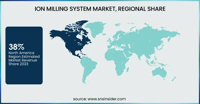
In 2023, North America dominated the ion milling system market, accounting for approximately 38% of the total revenue. This dominance is primarily driven by the presence of well-established semiconductor, aerospace, and medical research industries in the region, particularly in the United States. The U.S. has witnessed significant investment in nanotechnology, microelectronics, and advanced materials research, which has led to a growing demand for high-precision material analysis tools like ion milling systems. Additionally, the region is home to leading manufacturers and research institutions that continue to adopt cutting-edge technologies for failure analysis, sample preparation, and microscopy. Government initiatives supporting innovation in semiconductors, such as the CHIPS Act, have further strengthened the market’s foundation. Canada also contributes through its growing focus on materials science and healthcare R&D. With a strong infrastructure, skilled workforce, and ongoing technological advancements, North America is expected to maintain its leading position in the ion milling system market.
The Asia Pacific region is projected to be the fastest-growing market for ion milling systems during the forecast period from 2024 to 2032. This rapid growth is driven by increasing investments in semiconductor manufacturing, electronics, and materials science across key countries such as China, Japan, South Korea, and Taiwan. These nations are global leaders in chip fabrication, nanotechnology, and consumer electronics, all of which require high-precision sample preparation and surface analysis tools. China’s expanding semiconductor ecosystem and aggressive push for technological self-sufficiency, along with Japan’s advanced R&D capabilities and South Korea’s dominance in memory chip production, are fueling regional demand. Moreover, academic and industrial research institutions in the region are adopting ion milling systems for medical, materials, and energy research. The combination of government support, growing R&D activities, and the presence of leading tech manufacturers positions Asia Pacific as the fastest-growing region in the ion milling system market.
Get Customized Report as per Your Business Requirement - Enquiry Now
Major Players in Ion Milling System Market along with their Products:
-
4Wave Inc. (USA) – Offers ion beam deposition and milling systems for thin film applications.
-
AJA International Inc. (USA) – Provides customizable ion milling and sputtering tools for research and semiconductors.
-
Eden Instruments SAS (France) – Supplies ion beam etching equipment for precision surface analysis.
-
Gatan, Inc. (USA) – Specializes in precision ion polishing systems for electron microscopy sample prep.
-
Hitachi High-Technologies Corp. (Japan) – Produces advanced FIB systems and electron microscopes.
-
Intlvac Thin Film Corp. (Canada) – Develops ion beam etching and deposition tools for tech industries.
-
Leica Microsystems GmbH (Germany) – Manufactures EM sample prep and ion milling equipment.
-
Microfab Inc. (USA) – Provides FIB milling and microfabrication equipment.
-
Nano-Master, Inc. (USA) – Designs compact ion beam etch and sputter systems.
-
Nordiko Technical Services Ltd. (UK) – Offers ion beam milling and sputtering systems for analysis.
-
Oxford Instruments PLC (UK) – Delivers plasma and ion beam etching tools for nanotech and semiconductors.
-
Scia Systems GmbH (Germany) – Makes precision ion beam milling and trimming systems.
-
Scientific Vacuum Systems Ltd. (UK) – Supplies ion beam etching and deposition tools for labs.
-
Technoorg Linda Co. Ltd. (Hungary) – Offers ion beam milling systems for TEM sample prep.
-
Veeco Instruments Inc. (USA) – Provides high-performance ion beam etch systems.
List of key suppliers providing raw materials and components for the Ion Milling System Market:
-
Pravartaka Infotechnates (India)
-
Intlvac Thin Film Corporation (Canada)
-
Matsusada Precision (Japan)
-
MCube Technologies (India)
-
Plassys-Bestek (France)
-
PhotonExport (Spain)
-
Fraction Technologies Pte. Ltd. (Singapore)
-
AJA International Inc. (USA)
-
Leica Microsystems GmbH (Germany)
-
Hitachi High-Technologies Corporation (Japan)
Recent News:
-
5 Mar 2025, The ArBlade 5000 II/IM5000 by Hitachi High-Tech Europe is a high-performance broad ion beam system designed for rapid, high-quality cross-section and flat surface milling in electron microscopy, featuring a powerful Ar ion gun that delivers twice the milling speed for reduced processing time.
| Report Attributes | Details |
|---|---|
| Market Size in 2023 | USD 2.22 Billion |
| Market Size by 2032 | USD 4.78 Billion |
| CAGR | CAGR of 8.90% From 2024 to 2032 |
| Base Year | 2023 |
| Forecast Period | 2024-2032 |
| Historical Data | 2020-2022 |
| Report Scope & Coverage | Market Size, Segments Analysis, Competitive Landscape, Regional Analysis, DROC & SWOT Analysis, Forecast Outlook |
| Key Segments | • By Product Type(Cross-Section Milling, Flat Surface Milling) • By Electron Microscopy Type(Scanning Electron Microscope (SEM), Transmission Electron Microscope (TEM), Focused Ion Beam (FIB)) • By Sample Material(Ceramics, Polymers, Composites, Metals, Other Materials) • By Application(Semiconductor Manufacturing, Geological Institutes, Forensic Laboratories, Medical Research Institutes, Food Analysis, Other Applications) |
| Regional Analysis/Coverage | North America (US, Canada, Mexico), Europe (Eastern Europe [Poland, Romania, Hungary, Turkey, Rest of Eastern Europe] Western Europe] Germany, France, UK, Italy, Spain, Netherlands, Switzerland, Austria, Rest of Western Europe]), Asia-Pacific (China, India, Japan, South Korea, Vietnam, Singapore, Australia, Rest of Asia-Pacific), Middle East & Africa (Middle East [UAE, Egypt, Saudi Arabia, Qatar, Rest of Middle East], Africa [Nigeria, South Africa, Rest of Africa], Latin America (Brazil, Argentina, Colombia, Rest of Latin America) |
| Company Profiles | 4Wave Inc. (USA), AJA International Inc. (USA), Eden Instruments SAS (France), Gatan, Inc. (USA), Hitachi High-Technologies Corp. (Japan), Intlvac Thin Film Corp. (Canada), Leica Microsystems GmbH (Germany), Microfab Inc. (USA), Nano-Master, Inc. (USA), Nordiko Technical Services Ltd. (UK), Oxford Instruments PLC (UK), Scia Systems GmbH (Germany), Scientific Vacuum Systems Ltd. (UK), Technoorg Linda Co. Ltd. (Hungary), and Veeco Instruments Inc. (USA) are key players in the Ion Milling System Market. |
Get in Touch
