Scanning Electron Microscopes Market Size Analysis
Get more information on Scanning Electron Microscopes Market - Request Free Sample Report
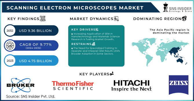
The Scanning Electron Microscopes Market Size was valued at USD 4.75 Billion in 2023, and is expected to reach USD 9.36 Billion by 2032, and grow at a CAGR of 9.77%.
The microscope is an essential equipment in various procedures of the manufacturing of semiconductor devices, including lithography, coating failure analysis, etc. Nowadays, the demand for scanning electron microscopes (SEMs) is growing just as rapidly in other parts of Asia, particularly countries like India and China where the semiconductor industry shows promising growth owing to outsourcing of electric equipment manufacturing.
Increased R&D spending in areas such as neurology, materials science, life sciences, and nanotechnology along with semi-conductor industries globally has propelled the market for advanced automated microscopes. For production as well, and to achieve high imaging resolution such as 0.1 nm they use different kinds of advanced technological tools which include Scanning Probe Microscopes (SPM), Analytical electron microscopes, etc. SEM is one among them where the user gets high Images with details matching the precision required in these manufacturing industries.
Nanotechnology is also used in various other areas like semiconductors, material sciences, and life sciences which are going to change the economy of countries. This has fueled the demand for public funding of research and development by government organizations and corporate enterprises. There is a huge demand for microscopes as they play an important role in the analysis of atomic-scale nanomaterials especially when it comes to industries such as pharmaceuticals, and medical devices along with several other verticals that are driving the global market for microscopy.
MARKET DYNAMICS:
Key Drivers:
-
Increasing Application of SEM In Nanotechnology and Materials Science Research Is Fueling Market Growth.
-
Continuous Innovations in SEM Technology, Such as Improved Resolution and Faster Imaging, Drive Demand Across Various Industries.
Restraints:
-
The Significant Upfront and Maintenance Costs Associated with Sems Can Be a Barrier for Smaller Research Institutions and Companies.
-
The Need for Specialized Training to Operate and Interpret SEM Results Limits Broader Adoption in Some Sectors.
Opportunity:
-
Growing Industrialization and Research Initiatives in Emerging Economies Present Opportunities for Market Expansion.
-
Developing SEM With AI-Driven Analysis and Automated Workflows Could Enhance Usability and Attract New Users.
KEY MARKET SEGMENTATION:
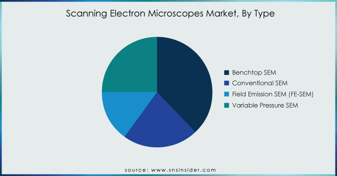
By Type
Field Emission SEM or FE-SEM led the scanning electron microscope (SEM) market owing to its benefits like high-resolution imaging and advanced technology with 38% of share in 2023. The unique ability of FE-SEMs to deliver excellent resolution provides detailed images that are important for many high-precision research or industrial requirements, as weakly present nanoscale structures can be seen clearly with other intricate surface features. The chain of performance comes from a field emission source creating an electron beam with higher spatial resolution and brilliance than ever before in SEM. Consequently, the FE-SEM is desperately needed in areas like material science and nanotechnology research to fully observe small features. While conventional SEMs are much more suitable for a variety of applications and thus yield a higher number in terms of demand, on account of their greater application–to–price-performance value ratio; the high-resolution detail-orientated imaging requirements embodied within FE-SEMs drive them toward an appearance dominant across said markets which are becoming increasingly focused upon technological adaptability.
Get Customized Report as per your Business Requirement - Request For Customized Report
REGIONAL ANALYSIS:
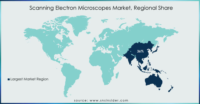
The rapid industrialization and high investments in the technology and research sectors within regions such as Asia Pacific make it the most prevalent market for scanning electron microscopes (SEMs) with a 36% share in 2023. The application areas like semiconductors, pharmaceuticals, and nanotechnologies which are the key sectors demanding advanced imaging tools such as SEMs have shown significant growth in this region. China, Japan, and South Korea are leading the way with technological developments and manufacturing breakthroughs that maintain their dominance in this region. High resolution and precise imaging are demanded by the electronics and automotive, burgeoning in Asia Pacific leading towards quality control or research among other applications which supports increased adoption of SEM as a part of analysis. Furthermore, growing research infrastructure and rising funding in scientific research are also expected to propel the growth of the SEM market. Because of this, Asia Pacific is the largest regional market for SEM as it offers an amalgamation of extensive industrial activities associated with considerable budget allocations in technology investment and its research expansion.
KEY PLAYERS:
The key market players are Bruker Corp., Danish Micro Engineering (DME), Thermo Fisher Scientific, Hitachi High Technologies Corp., JEOL Ltd., Leica Microsystems, Nanoscience Instruments, Inc., Nikon Corp., Olympus Corp., Carl Zeiss & other players.
RECENT DEVELOPMENTS
-
Thermo Fisher Scientific released the Thermo Scientific Phenom Pharos G2 Desktop Field Emission Gun Scanning Electron Microscope (FEG-SEM) in July 2021. The device was even able to differentiate between sizes, shapes, and chemical compositions of nanoparticles across a wide range with this product.
-
Thermo Fisher Scientific Inc., an American provider of scientific instrumentation reported the acquisition of PPD, Inc. in December 2021 for USD 17.4 billion.
|
Report Attributes |
Details |
|
Market Size in 2023 |
US$ 4.75 Billion |
|
Market Size by 2032 |
US$ 9.36 Billion |
|
CAGR |
CAGR of 9.77% From 2024 to 2032 |
|
Base Year |
2023 |
|
Forecast Period |
2024-2032 |
|
Historical Data |
2020-2022 |
|
Report Scope & Coverage |
Market Size, Segments Analysis, Competitive Landscape, Regional Analysis, DROC & SWOT Analysis, Forecast Outlook |
|
Key Segments |
•By Type (Benchtop SEM, Conventional SEM, Field Emission SEM (FE-SEM) & Variable Pressure SEM) |
|
Regional Analysis/Coverage |
North America (US, Canada, Mexico), Europe (Eastern Europe [Poland, Romania, Hungary, Turkey, Rest of Eastern Europe] Western Europe] Germany, France, UK, Italy, Spain, Netherlands, Switzerland, Austria, Rest of Western Europe]), Asia Pacific (China, India, Japan, South Korea, Vietnam, Singapore, Australia, Rest of Asia Pacific), Middle East & Africa (Middle East [UAE, Egypt, Saudi Arabia, Qatar, Rest of Middle East], Africa [Nigeria, South Africa, Rest of Africa], Latin America (Brazil, Argentina, Colombia, Rest of Latin America) |
|
Company Profiles |
Bruker Corp., Danish Micro Engineering (DME), Thermo Fisher Scientific, Hitachi High Technologies Corp., JEOL Ltd., Leica Microsystems, Nanoscience Instruments, Inc., Nikon Corp., Olympus Corp., Carl Zeiss & other players |
|
Key Drivers |
•Increasing Application of SEM In Nanotechnology and Materials Science Research Is Fueling Market Growth. |
|
RESTRAINTS |
•The Significant Upfront and Maintenance Costs Associated with Sems Can Be a Barrier for Smaller Research Institutions and Companies. |
Frequently Asked Questions
Ans: The Scanning Electron Microscopes Market was valued at USD 4.75 Billion in 2023.
Ans: The expected CAGR of the Global Scanning Electron Microscopes Market during the forecast period is 9.77%
Ans: Life Science held the largest share in the Scanning Electron Microscopes Market in 2023.
Ans: The Scanning Electron Microscopes Market will be valued at USD 9.36 Billion in 2032.
Ans: The Asia Pacific led Scanning Electron Microscopes Market.
Get in Touch
