Thin-Film Encapsulation Market Report & Overview:
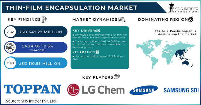
The Thin-Film Encapsulation Market size was valued at USD 110.53 million in 2023 and is expected to grow to USD 549.27 million by 2032 and grow at a CAGR Of 19.5% over the forecast period of 2024-2032. Increasing use of thin-film barriers in flexible and organic electronic devices is the major driver for the growth of the market. Another important factor driving market growth is the combination of flexible OLED displays into smartphones and also smart wearables. Strides in automation, manufacturing efficiencies, and supply chain management have also been important enablers of growth across regions.
Get More Information on Thin-Film Encapsulation Market- Request Sample Report
Thin-Film Encapsulation Market Dynamics
Drivers:
-
Growth of Thin-Film Encapsulation in Flexible Electronics and OLED Technologies
Demand for flexible electronics, powered by flourishing of flexible oled displays in smartphones, wearables and consumer electronics, is driving the thin-film encapsulation (tfe) market because of this property, tfe is critical for preventing environmental damage to oleds and organic electronics, such as moisture and oxygen. Organics are also being used in solar cells to improve efficiency and more recently device protection, with organic-inorganic hybrid thin-film encapsulation being used to boost stability. Technological advancements, including atomic layer deposition (ALD) and inkjet printing, are expected to fuel market growth. The rise of wearable devices and flexible OLEDs further strengthens TFE's market position, while automotive applications, like OLED lighting, expand its reach. However, flexible glass technology poses a challenge as it may replace TFE, but the technology remains vital for flexible OLEDs' future.
Restraints:
-
Material shortages of key compounds can break supply chains, raise costs, and slow the growing thin-film encapsulation technology.
Material shortages pose a significant challenge for the Thin-Film Encapsulation (TFE) market as TFE involves the use of specialized materials, including metal oxides and other high-performance compounds. A disruption to the supply chains of these materials would cause higher production costs and delays. For instance, the use of metal oxides, key to forming moisture barriers in TFE layers, could be impacted, leading to constraints on supply of one of the essential features as well. the Thin-film Encapsulation s has potential to delay mass manufacturing and reduce the scalability of TFE applications in key areas such as flexible electronics, OLED displays and bioelectronics.
Opportunities:
-
Bioelectronics integration in thin-film encapsulation offers a key opportunity as wearable devices and biosensors create new markets for TFE technologies.
The growing field of bioelectronics, including wearable health devices, biosensors, and implantable electronics, is increasingly dependent on thin-film encapsulation (TFE) technologies for protecting delicate components from environmental damage such as moisture and oxygen. TFE provides an ideal solution for bioelectronics due to its flexibility, durability, and lightweight nature, ensuring the longevity of sensitive devices. With advancements in TFE technologies, such as atomic layer deposition (ALD) and inkjet printing, manufacturers are enhancing performance while reducing costs. These innovations are expanding the application of TFE in bioelectronics, offering significant growth potential in the sector.
Challenges:
-
Material durability challenges for Thin-Film Encapsulation involve ensuring long-term reliability, resistance to environmental factors, and flexibility.
One of the significant challenges for the Thin-Film Encapsulation market is ensuring the long-term durability of materials used in encapsulation. The TFE technology must offer reliable protection against environmental factors such as moisture and oxygen while maintaining the necessary flexibility for flexible electronic devices like OLED displays and wearable technologies. Materials like metal oxides used in TFE structures are susceptible to degradation over time due to exposure to these elements, which can affect their protective properties. The above elements and thus the performance in terms of protection deteriorates. The researchers are exploring new materials and advanced deposition methods, such as atomic layer deposition, to overcome this problem, but these have yet to be incorporated into large-scale production. For the growth of the market, a trade-off needs to be maintained between durability vs flexibility at a lower cost.
Thin-Film Encapsulation Market Segment Analysis:
By Technology
Plasma-enhanced chemical vapor deposition (PECVD) dominates the Thin Film Encapsulation (TFE) market, holding a significant share of around 36% in 2023. This technique is preferred because it allows for the deposition of thin films with high-quality attributes, such as improved moisture resistance, greater flexibility, and greater durability; features, which are important for OLEDs and other sensitive electronics. PECVD growth is propelled by versatility, where it is applied in diverse industries, such as electronics, automotive and bioelectronics. Its cost-effective and scalable process also contributes to its widespread adoption, making it a key technology in advancing TFE applications and ensuring the longevity of electronic devices exposed to environmental factors.
Atomic Layer Deposition (ALD) is the fastest-growing segment in the Thin Film Encapsulation (TFE) market over the forecast period from 2024 to 2032. ALD offers precise control over film thickness, uniformity, and composition, making it ideal for advanced encapsulation applications in OLED displays, bioelectronics, and flexible electronics. Its being fueled by its capability to provide conformal coatings with outstanding oxygen and moisture barrier performance, even on complex topographies. ALD is easily scalable and further developments of precursor and deposition methods will contribute to the increasing penetration of this technology into the market, making it one of the dominant technologies used in TFE applications.
By Application
The flexible OLED display segment dominated the Thin Film Encapsulation market, accounting for around 49% in 2023. This segment's growth is driven by the increasing back of rising demand for lighter, thinner and flexible display from smartphones, wearables and consumer electronics. Flexible OLED displays provide enhanced image quality, high-energy efficiency, and the possibility of curved or foldable designs, which are very appealing to consumers. TFE technology is critical in protecting OLED materials from environmental damage like moisture and oxygen, ensuring long-term durability.
The Thin-Film Photovoltaics (TFPV) segment is the fastest-growing segment in the Thin Film Encapsulation market over the forecast period 2024-2032. Driven by the increasing adoption of renewable energy sources and advancements in solar technology, thin-film photovoltaics offer advantages such as flexibility, lightweight, and cost-efficiency compared to traditional solar panels. TFE technology plays a crucial role in protecting thin-film solar cells from environmental factors like moisture and oxygen, enhancing their durability and efficiency.
Need any customization research on Thin-Film Encapsulation Market - Enquiry Now
Thin-Film Encapsulation Market Regional Analysis
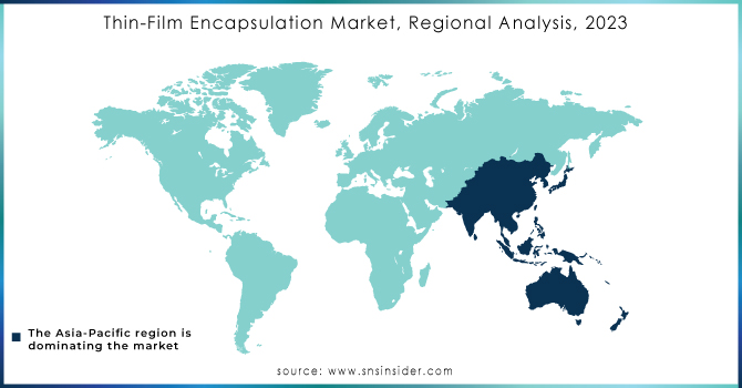
The Asia-Pacific region dominates the Thin-Film Encapsulation market with around 50% market share in 2023, driven by rapid advancements in electronics, renewable energy, and OLED technology. Countries like China, Japan, South Korea, and India are key contributors to this growth China is beating the world in organic light-emitting diode (OLED) production and solar cell technologies, while Japan and South Korea are dominant in flexible electronics and display technologies. Its dominance in the TFE market is further strengthened by the region's established manufacturing infrastructure, ability to manufacture products in large quantities, and increasing investments in the renewable energy technology sector. Additionally, the rising demand for wearable devices and flexible displays in Asia-Pacific supports TFE's widespread adoption.
North America is the fastest-growing region in the Thin-Film Encapsulation (TFE) market over the forecast period 2024-2032. The United States, in particular, leads in the adoption of advanced display technologies, bioelectronics, and flexible OLEDs, driving demand for TFE solutions. The region's robust research and development sector, coupled with significant investments in renewable energy and flexible electronics, is accelerating market growth. Additionally, North America has a strong base of technological innovation in atomic layer deposition (ALD) and other advanced deposition techniques. Key market players and the region's emphasis on sustainability and green technologies also make it ideally suited for significant growth in the TFE market.
Thin-Film Encapsulation Market Key Players
Some of the major key players in Thin Film Encapsulation Market along with their product:
-
Samsung SDI Co., Ltd. (South Korea) – (Lithium-ion batteries, OLED materials)
-
LG Chem (South Korea) – (Lithium-ion batteries, OLED materials)
-
Universal Display Corporation (USA) – (OLED technologies, phosphorescent materials)
-
3M (USA) – (Optical films, adhesive materials)
-
Applied Materials, Inc. (USA) – (Semiconductor processing equipment, display technologies)
-
Meyer Burger Technology AG (Switzerland) – (Solar cell production equipment)
-
Toray Industries, Inc. (Japan) – (Advanced materials, OLED displays)
-
Toppan Inc. (Japan) – (Display films, packaging materials)
-
Ergis Group (Poland) – (Flexible packaging films)
-
Veeco Instruments Inc. (USA) – (Deposition equipment, LED materials)
-
Kateeva (USA) – (Inkjet printing for OLED displays)
-
tesa (Germany) – (Adhesive tapes, display bonding solutions)
-
Ajinomoto Fine-Techno Co., Inc. (Japan) – (Photomasks, OLED materials)
-
Coat-X (Germany) – (Thin film deposition equipment)
-
Borealis AG (Austria) – (Polyolefins, specialty plastics)
-
OLED – (Organic light-emitting diode technology, display and lighting panels)
List of suppliers for the thin-film market who provide raw material and Component:
-
Mitsui Chemicals, Inc.
-
Dow Inc.
-
BASF
-
DuPont
-
Toray Industries, Inc.
-
Samsung SDI Co., Ltd.
-
LG Chem
Recent Development
-
28 August 2024, LG Display is exploring new ways to thin down foldable panels, trying to use black pixel define layer (PDL) samples that it purchased from Mitsubishi and other suppliers. This ingredient is important for enabling the application of CoE format technology, replacing the polarizing layer in the OLED panels, with a black PDL instead of the orange PDL normally used, will increase the efficiency of foldable OLED displays and thinness.
-
24 November 2024, OLED technology has focused on improving the longevity and efficiency of OLED panels, with significant advancements in Thin Film Encapsulation (TFE) technology to protect against moisture and oxygen damage. And companies such as Kateeva have led the way with inkjet printing of organic TFE (thin film encapsulation) layers, while advanced inorganic, i.e., glassy, layers are coming in to increase effectiveness and prolong the life of the OLED, particularly valuable in flexible screens and wearables.
-
10 January 2025, Samsung to introduce Color-filter-on-thin-film-encapsulation (CoE) to next Galaxy S26 Ultra, planned for 2026 Already utilized in Samsung foldables including the Galaxy Z Fold 3 and Z Fold 6, this tech features a revamped layout that places color filters directly above the new thin encapsulation layer, which improves screen efficiency, brightness, and other aspects of screen quality. With this, the S26 Ultra
| Report Attributes | Details |
| Market Size in 2023 | USD 110.53 Million |
| Market Size by 2032 | USD 549.27 Million |
| CAGR | CAGR of 19.5% From 2024 to 2032 |
| Base Year | 2023 |
| Forecast Period | 2024-2032 |
| Historical Data | 2020-2022 |
| Report Scope & Coverage | Market Size, Segments Analysis, Competitive Landscape, Regional Analysis, DROC & SWOT Analysis, Forecast Outlook |
| Key Segments | • By Technology (Plasma-enhanced chemical vapor deposition (PECVD), Atomic layer deposition (ALD), Inkjet Printing, Vacuum Thermal Evaporation (VTE), Other Technologies) • By Application (Flexible OLED Display, Thin-Film Photovoltaics, Flexible OLED Lighting, Other Applications) |
| Regional Analysis/Coverage | North America (US, Canada, Mexico), Europe (Eastern Europe [Poland, Romania, Hungary, Turkey, Rest of Eastern Europe] Western Europe] Germany, France, UK, Italy, Spain, Netherlands, Switzerland, Austria, Rest of Western Europe]), Asia Pacific (China, India, Japan, South Korea, Vietnam, Singapore, Australia, Rest of Asia Pacific), Middle East & Africa (Middle East [UAE, Egypt, Saudi Arabia, Qatar, Rest of Middle East], Africa [Nigeria, South Africa, Rest of Africa], Latin America (Brazil, Argentina, Colombia, Rest of Latin America) |
| Company Profiles | Samsung SDI Co., Ltd. (South Korea), LG Chem (South Korea), Universal Display Corporation (USA), 3M (USA), Applied Materials, Inc. (USA), Meyer Burger Technology AG (Switzerland), Toray Industries, Inc. (Japan), Toppan Inc. (Japan), Ergis Group (Poland), Veeco Instruments Inc. (USA), Kateeva (USA), tesa (Germany), Ajinomoto Fine-Techno Co., Inc. (Japan), Coat-X (Germany), Borealis AG (Austria).,OLed. |
Frequently Asked Questions
Ans: The Asia-Pacific is dominating in Thin-film Encapsulation market.
Ans: Thin-film Encapsulation Market size was valued at USD 110.53 million in 2023.
Ans: The Thin-film Encapsulation Market is estimated to reach USD 549.27 million by 2032.
Ans: The key driver for the Thin-Film Encapsulation market is the growing demand for flexible electronics, particularly in OLED displays and renewable energy applications.
Ans: Thin-film Encapsulation Market is anticipated to expand by 19.5% from 2024 to 2032.
Get in Touch
