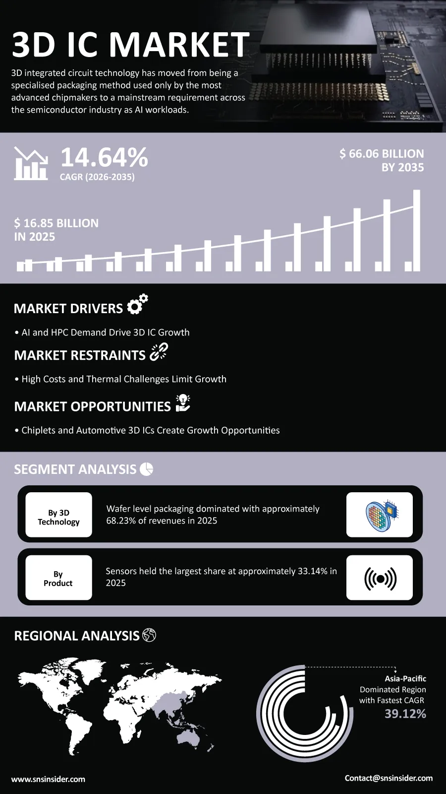
The global 3D IC Market is entering a new phase of accelerated growth as semiconductor manufacturers embrace advanced packaging technologies to meet rising demand for artificial intelligence, high-performance computing, and next-generation consumer electronics. According to a recent study by SNS Insider, the global 3D IC Market size valued at USD 16.85 billion in 2025, is anticipated to grow to USD 66.06 billion by 2035, registering a CAGR of 14.64% over the 2026–2035 forecast period.
Growing requirements for enhanced data processing speeds, greater memory bandwidths, and better energy efficiencies have been driving chip manufacturers towards vertically-integrated semiconductor designs. With traditional chip scaling becoming more and more challenging, 3D integration appears to be a realistic approach to providing performance upgrades within a smaller physical footprint.
The development of advanced semiconductor packing solutions for AI processors, cloud computing systems, autonomous cars, and future-generation communications networks has become an important goal for technology providers. Further advancements in the field of semiconductors manufacturing will contribute to even greater commercialization of 3D ICs during the next decade.
To Get Detailed Insights on the 3D IC Market – Request a Sample Report
AI Infrastructure Expansion Creates Significant Growth Opportunities
There has been significant growth in the deployment of artificial intelligence platforms and large data centers, and this will have an impact on the needs in the semiconductor industry. The use of advanced processors means that more bandwidth and reduced latency will be needed, which makes 3D integration very suitable to provide better computing performance while minimizing energy use.
On the other hand, the increasing use of chiplet design architecture helps semiconductor companies in combining specific processing capabilities into a package. This provides more flexibility in production as well as quicker development of products in AI, automobile, industrial automation, and telecoms.
Government initiatives supporting domestic semiconductor manufacturing and advanced packaging capacity are also creating new opportunities for technology providers, equipment manufacturers, and semiconductor foundries worldwide.
Key Market Insights Highlight Shifting Demand Patterns
By 3D technology, wafer-level packaging accounted for approximately 68.23% of global market revenue in 2025, supported by its widespread deployment in smartphones, wearable devices, and other space-constrained electronic products. System integration is projected to register the fastest growth through the forecast period as heterogeneous chiplet assembly gains momentum across AI, high-performance computing, and automotive applications.
Based on product, sensors segment led the market with approximately 33.14% of market revenue in 2025 due to expanding adoption across smartphones, autonomous vehicles, industrial equipment, and IoT devices. Memory devices are forecast to experience the fastest growth as demand for high-bandwidth memory continues to increase across AI accelerators and cloud computing platforms.
By application, ICT and telecommunication generated approximately 34.65% of market revenue in 2025, reflecting continued investments in 5G infrastructure, networking equipment, and high-speed communication systems. Consumer electronics are projected to emerge as the fastest-growing application segment as premium smartphones, gaming devices, and wearable technologies increasingly incorporate advanced 3D IC architectures.
Advanced Packaging Technologies Continue to Transform Semiconductor Design
A trend towards advanced packaging techniques, which enhance the processing capabilities along with energy efficiency, is evident within the semiconductor industry. With hybrid bonding, wafer-level packaging, and high-density interconnects, it becomes possible to create smaller and more efficient semiconductor products that can operate under more complex workload conditions.
Widening usage of 3D IC technology in automotive electronics, image sensors, industrial automation, and edge computing systems is creating additional opportunities for the semiconductor market. The semiconductor manufacturers remain focused on process development to enhance yields, heat dissipation, and packaging reliability.
North America Leads the Market, While Asia Pacific Grows at 15.45% CAGR
The North American market is anticipated to retain its position as the leading regional market throughout the forecast period owing to the existence of some major semiconductor vendors, investment in AI infrastructure, and increasing advanced packaging operations in the region. Government-sponsored semiconductor manufacturing activities are also set to improve the competitiveness of the region in advanced chip manufacturing.
On the other hand, Asia Pacific is likely to emerge as the fastest growing regional market with a CAGR of 15.45% over the forecast period. Competent semiconductor manufacturing facilities, increasing foundries investments, growing AI infrastructure implementation, and growing consumer electronic products manufacturing in the region is set to drive the regional 3D IC market.
As semiconductor supply chains continue evolving to meet future computing requirements, regional investments in advanced packaging technologies are expected to accelerate significantly.
Industry Participants Focus on Advanced Packaging Innovation
The competitive landscape remains highly dynamic as semiconductor companies continue expanding advanced packaging capacity and developing next-generation integration technologies. Manufacturers are investing in hybrid bonding, high-bandwidth memory integration, chiplet architectures, and advanced interconnect solutions to improve performance while supporting increasingly complex semiconductor designs.
Key companies operating in the global 3D IC Market include IBM, ASE Technology Holding Co. Ltd., STMicroelectronics, Samsung, Taiwan Semiconductor Co. Ltd., Toshiba Corporation, Micron Technology Inc., MonolithIC 3D Inc., Intel Corporation, Tezzaron, Amkor Technology, Jiangsu Changdian Technology Co. Ltd., United Microelectronics Corporation, Advanced Micro Devices Inc., ANSYS Inc., Cadence Design Systems Inc., EV Group (EVG), SUSS MicroTec SE, Siliconware Precision Industries Co. Ltd., and Camtek.
An SNS Insider analyst Sushant Kadam commented, “The rapid evolution of artificial intelligence, cloud computing, and advanced semiconductor packaging is creating substantial opportunities for 3D IC technologies. Companies investing in next-generation packaging platforms, heterogeneous integration, and manufacturing innovation will be well positioned to support the future demands of high-performance computing and intelligent electronic systems.”
About the Author

Get in touch