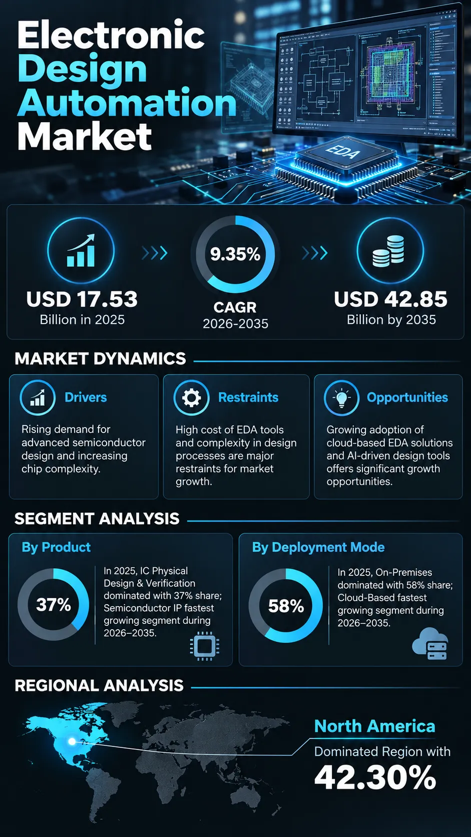
The Electronic Design Automation Market is expected to grow steadily since the semiconductor industry and tech companies continue to develop advanced chip designs. According to a recent study by SNS Insider, the global Electronic Design Automation (EDA) Market size valued at USD 17.53 billion in 2025, is anticipated to grow to USD 42.85 billion by 2035, registering a CAGR of 9.35% over the 2026–2035 forecast period.
Due to the rapid growth of the usage of artificial intelligence, Internet of Things (IoT), telecommunications, and computing, the process of semiconductor design becomes more complicated. Given the smaller and denser design of the chip architecture, developers make use of software for the management of the process of design accuracy and efficiency.
Moreover, the development of the fabless semiconductor business model and investments into chip production open up new perspectives for EDA providers. Finally, cloud computing and AI-enabled design bring changes into the way design resources are utilized.
To Get Detailed Insights on the Electronic Design Automation Market – Request a Sample Report
Semiconductor Complexity Continues to Create New Growth Opportunities
The shift toward advanced node processes and more complex SoCs is driving the need for technologies that will be able to handle complex design and verification processes. Semiconductor companies are looking for technologies that will help them overcome development roadblocks while achieving complex requirements with regards to performance, power, and reliability.
Design automation utilizing artificial intelligence is becoming one of the areas for investment as engineering teams try to automate their processes and speed up development processes. Cloud-based EDA solutions are getting more recognition because of scalability and collaboration opportunities that they offer without having to invest heavily in dedicated infrastructures.
Rising semiconductor investments in such sectors as automotive, telecommunications, consumer electronics, and industrial electronics are projected to drive the addressable market of EDA technologies even further.
Key Market Insights Highlight Shifting Demand Patterns
By product, IC Design & Verification is anticipated to contribute about 37 percent to the world market revenue in 2025 due to the growing complexities of the integrated circuits and the need for verification of their designs. The Semiconductor Intellectual Property is forecasted to be the most rapidly growing sector until 2035 owing to the reusable design blocks that assist designers save their efforts, money, and time.
Based on deployment mode, on-premise solutions are estimated to account for 58% of revenue in 2025 on the back of requirements for direct infrastructure control and data protection. Cloud EDA solutions will witness the highest CAGR due to an increased demand among semiconductor startups and mature firms for scalable computing resources, collaboration tools, and engineering tools.
In terms of application, microprocessors and microcontrollers are predicted to account for 41% revenue share in 2025, owing to their extensive use in electronic systems and devices. Memory Management Units (MMUs) are anticipated to grow at the highest rate, driven by the increasing need for advanced computing solutions and semiconductors.
By end user, the consumer electronics sector is expected to contribute to 39% of the market’s revenue share by 2025. The automotive end-use sector is likely to experience the highest growth rate due to the increasing requirement of semiconductor technology in electric vehicles, autonomous driving platforms, ADAS, and connected vehicles.
AI and Cloud Technologies Reshape Chip Design Workflows
AI and machine learning have begun to be used by EDA vendors in optimizing the designs, verifying them, and in the engineering process. They may help detect problems with the design early and perform automation of some development stages as well as use of engineering resources more efficiently.
Access to advanced computing is also expanding due to the cloud infrastructure. This combination of cloud EDA, collaboration, and AI-enabled engineering creates a more flexible development environment for businesses that design complicated semiconductor devices.
North America Leads EDA Market with 42.30% Share as Asia Pacific Grows at 10.10% CAGR
The North American region is predicted to have 42.30% share of Electronic Design Automation Market revenue in 2025, driven by robust semiconductor industry, presence of EDA suppliers, research & development, and initiatives toward artificial intelligence, 5G, and high-performance computing.
The Asia-Pacific region is forecasted to be the fastest-growing regional market, experiencing CAGR of 10.10% till 2035. Development in semiconductor fabrication facilities across China, Taiwan, South Korea, Japan, and India, along with increasing electronics demands and advancements in chip design, will help in the adoption of the market in the region.
The European region is gaining due to automotive and industrial technology strengths, and Latin America is evolving because of the process of digitalization and increased electronics adoption. The Middle East & Africa region is receiving momentum from telecommunications, smart infrastructure, and industrial automation projects.
Industry Participants Accelerate AI-Driven EDA Innovation
The competitive scenario continues to revolve around building capabilities in software, enhancing the IP of semiconductor, and embedding AI into the design process of chips. Some leading firms are also making investments in the cloud and collaborating strategically in order to meet increasing technical needs for semiconductor production.
Key companies operating in the global Electronic Design Automation Market include Synopsys, Cadence Design Systems, Siemens EDA, ANSYS, Keysight Technologies, Zuken, Altair Engineering, Autodesk, Altium, Mentor Graphics, Silvaco, AWR Corporation, Magma Design Automation, Dassault Systèmes, National Instruments, ARM Holdings, Rambus, Xilinx, Intel, and Broadcom.
An SNS Insider analyst Sushant Kadam commented, “The increasing sophistication of semiconductor architectures is creating sustained demand for more intelligent and scalable design automation capabilities. The convergence of AI-assisted engineering, cloud computing, advanced-node development, and expanding semiconductor investments is opening significant opportunities for EDA providers across both established and emerging technology markets.”About the Author

Get in touch