3D IC Market Report Scope & Overview:
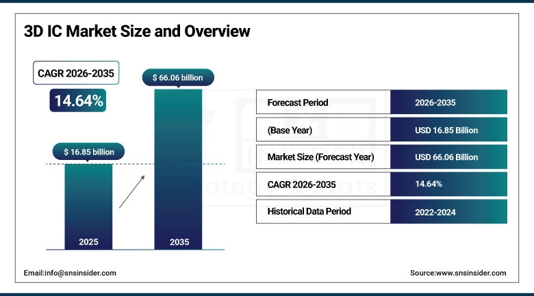
The 3D IC market was valued at USD 16.85 billion in 2025 and is expected to reach USD 66.06 billion by 2035, growing at a CAGR of 14.64% from 2026–2035.
3D integrated circuit technology has moved from being a specialised packaging method used only by the most advanced chipmakers to a mainstream requirement across the semiconductor industry as AI workloads, high-performance computing platforms, and 5G communications demand capabilities that flat, two-dimensional chip designs can no longer deliver at commercially viable power budgets. A 3D IC stacks two or more layers of active circuitry in a single package, connecting them vertically through an array of Through-Silicon Vias, micro-bumps, or direct hybrid bonds rather than routing signals across a conventional printed circuit board. This arrangement dramatically shortens the electrical path between memory and logic, which cuts latency and power consumption while sharply increasing the bandwidth available per unit of silicon area. The result is a package that is simultaneously smaller, faster, and more energy-efficient than an equivalent two-dimensional solution, a combination that is particularly valuable in mobile devices constrained by battery life and thermal limits, in data centres where electricity costs run into hundreds of millions of dollars annually, and in automotive electronics where reliability under harsh conditions is non-negotiable.
The market encompasses the full range of 3D packaging architectures including wire-bonded stacked memories, wafer-level fan-out packages, interposer-based 2.5D assemblies, and fully monolithic 3D structures where transistors are fabricated directly on top of one another. Leading semiconductor foundries and outsourced assembly and test providers have invested heavily in Through-Silicon Via etching, wafer thinning, precision bonding equipment, and inspection tools to bring these structures into reliable mass production. AI accelerator chips from NVIDIA, AMD, and Google now routinely integrate high-bandwidth memory stacks, and the commercial success of these devices has validated 3D integration at scale in ways that are drawing even cost-sensitive consumer electronics customers toward advanced packaging.
Market Size and Forecast
-
Market Size in 2026E: USD 19.32 Billion
-
Market Size by 2035: USD 66.06 Billion
-
CAGR (2026–2035): 14.64%
-
Fastest Growing Region: Asia Pacific
-
Largest Region: North America
To Get More Information On 3D IC Market - Request Free Sample Report
3D IC Market Trends
-
Rising adoption of hybrid bonding in advanced AI and HPC chip packages is replacing micro-bump interconnects, delivering higher connection density per unit area, lower resistance, and direct metal-to-metal contacts that eliminate the solder collapse risks associated with fine-pitch bumping.
-
Increasing use of 3D IC packaging for high-bandwidth memory in AI accelerators and graphics processors is driving foundry capacity expansion at TSMC, Samsung, and SK Hynix as cloud vendors accelerate their AI infrastructure build-out.
-
Growing integration of MEMS sensors, image sensors, and application processors in a single stacked package is gaining traction in smartphones, wearables, and autonomous vehicle perception modules seeking smaller form factors.
-
Expanding automotive electronics applications for 3D ICs include radar, LiDAR, and advanced driver assistance processors where the combination of high compute density and thermal efficiency matches demanding in-vehicle requirements.
-
Increasing government investment in domestic semiconductor advanced packaging capacity in the United States, Europe, and Japan is accelerating infrastructure deployment and expanding the supplier base for 3D IC manufacturing outside Taiwan and South Korea.
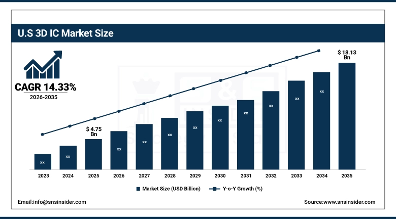
The U.S. 3D IC Market Outlook
The U.S. 3D IC Market was valued at approximately USD 4.75 billion in 2025 and is expected to reach approximately USD 18.13 billion by 2035, growing at a CAGR of 14.33% over the 2026–2035 forecast period, supported by strong domestic demand from AI chip designers, data-centre operators, defence electronics programmes, and the expanding CHIPS Act-funded semiconductor manufacturing base.
The United States leads the global 3D IC market through the combination of world-class semiconductor design companies headquartered domestically, including Intel, Micron, Qualcomm, NVIDIA, AMD, and Apple, with access to advanced packaging services through foundry partners and a domestic outsourced semiconductor assembly and test base that is growing rapidly as CHIPS Act funding flows into greenfield facilities. The Department of Defense's sustained interest in radiation-hardened 3D IC solutions for satellite and airborne systems creates a premium-price demand segment that justifies advanced process investment beyond what commercial economics alone would support. NSF and DARPA co-investment in academic and national laboratory 3D integration research maintains the pipeline of packaging innovation talent and process knowledge that commercial companies draw upon.
The CHIPS and Science Act's allocation of approximately USD 39 billion in manufacturing incentives and USD 13 billion for research and workforce development is creating the largest single surge in domestic advanced packaging capacity in decades, directly reinforcing the United States' competitiveness in 3D IC manufacturing and design.
3D IC Market Segment Analysis
-
By 3D Technology, wafer level packaging dominated with approximately 68.23% of revenues in 2025 owing to its widespread adoption in miniaturised consumer and mobile devices. System integration is the fastest-growing sub-segment driven by heterogeneous chiplet assembly for AI, HPC, and automotive applications.
-
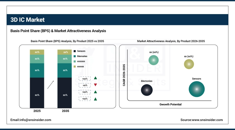
By Product, sensors held the largest share at approximately 33.14% in 2025 due to their broad adoption in smartphones, autonomous vehicles, and IoT. Memories are the fastest-growing segment driven by surging demand for high-bandwidth memory in AI accelerator and cloud computing platforms.
-
By Application, ICT/telecommunication dominated at approximately 34.65% share in 2025 fuelled by high-speed networking, 5G infrastructure, and data transport capacity needs. Consumer electronics is the fastest-growing application driven by premium smartphones, smart wearables, and gaming systems adopting 3D ICs for performance and battery life improvements.
-
By Component, through silicon vias held the largest share at approximately 46.32% in 2025 as they are the established vertical interconnect technology offering high bandwidth and low power. Through glass vias are the fastest-growing component segment owing to superior electrical properties and the progression of next-generation semiconductor packaging.
By 3D Technology, Wafer level packaging dominates, system integration is expected to grow fastest
Wafer level packaging retained the largest share of the 3D IC market in 2025 at approximately 68.23%, reflecting its established position as the preferred approach for high-volume consumer electronics and mobile applications where achieving the smallest possible footprint at a competitive cost per unit is the central engineering objective. The technique eliminates the conventional die separation step, processes chips collectively at the wafer level, and produces packages with near chip-scale dimensions that are well matched to the interior space constraints of smartphones, smartwatches, and wireless earbuds. Continuous improvement in fan-out wafer-level packaging yield rates and the expansion of embedded die options within wafer-level architectures are extending the technology into more demanding automotive and industrial applications.
System integration is the fastest-growing 3D Technology segment at a CAGR of 14.79% through 2033, reflecting the semiconductor industry's shift toward chiplet-based design strategies where compute, memory, I/O, and specialised accelerator functions are manufactured separately on their optimal process nodes and then assembled into a single heterogeneous package. The commercial success of AMD's EPYC and Ryzen processors using 3D V-Cache, and TSMC's CoWoS and SoIC platforms for packaging AI accelerators with high-bandwidth memory stacks, has demonstrated that system integration can deliver competitive cost and performance advantages over monolithic chip scaling.
By Product, sensors dominate, memories are expected to grow fastest
Sensors held the leading product position with approximately 33.14% of 3D IC Market revenues in 2025, reflecting the central role of image sensors, MEMS microphones, pressure sensors, and environmental sensors in the smartphones, wearables, autonomous vehicles, and smart home devices that collectively represent the world's largest market for packaged semiconductors. 3D stacking of sensor elements with dedicated signal-processing logic in a single compact package delivers the combination of sensitivity, speed, and physical compactness that premium mobile and automotive sensor applications require, and increasing sensor integration within a single stacked package is displacing discrete board-mounted solutions across a widening range of form-factor-constrained applications.
Memories are the fastest-growing product segment at a CAGR of 15.33% through 2033, driven by the insatiable bandwidth and capacity demands of AI training and inference workloads that conventional planar memory architectures cannot satisfy at acceptable power levels. The successful commercial deployment of High Bandwidth Memory stacks in NVIDIA's Hopper and Blackwell GPU generations, and AMD's Instinct MI series accelerators, has established 3D-stacked memory as the de facto standard for frontier AI hardware. Exponential growth in data centre AI compute investment, combined with the adoption of AI features in smartphones and edge devices, is sustaining rapid volume growth in high-bandwidth memory and in the stacked NAND and DRAM solutions used in high-performance storage and compute applications.
By Application, ICT/telecommunication dominates, consumer electronics is expected to grow fastest
ICT/telecommunication retained the dominant application position with approximately 34.65% of 3D IC market revenues in 2025, reflecting the foundational dependence of 5G base station radio units, optical networking line cards, data centre switching fabrics, and cloud computing processors on high-performance semiconductor packages capable of handling the combination of high data rates, low latency requirements, and demanding thermal environments that define modern communications infrastructure. Network switch ASICs, digital signal processors for 5G massive MIMO antenna arrays, and high-speed serialiser-deserialiser interfaces for optical modules all benefit directly from the bandwidth and latency improvements that 3D integration delivers relative to conventional two-dimensional packaging.
Consumer electronics is the fastest-growing application segment at a CAGR of 15.92% through 2033, driven by smartphone OEMs and wearable device manufacturers seeking to differentiate on camera performance, processing speed, battery life, and physical compactness in an intensely competitive market. Apple's proprietary system-in-package integration in AirPods and Apple Watch, combined with Samsung's and Qualcomm's roadmaps for increasingly integrated 3D mobile processor packages, is establishing advanced 3D IC packaging as a standard feature of premium consumer electronic products. The rapid consumer adoption of AI-powered photography, on-device language model inference, and augmented reality features is creating new performance requirements that are accelerating the transition of mainstream smartphone chips toward 3D architectures.
Regional Analysis:
|
Region |
Major Country |
Share within Region, 2025 (%) |
|---|---|---|
|
North America |
United States |
82% |
|
Europe |
Germany |
28% |
|
Asia Pacific |
Taiwan |
52% |
|
Middle East & Africa |
UAE |
24% |
|
Latin America |
Brazil |
38% |
North America 3D IC Market Insights
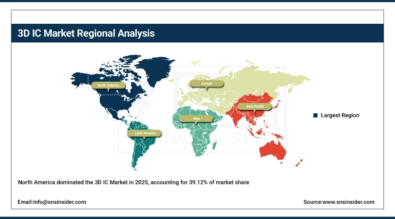
North America dominated the global 3D IC market in 2025 with approximately 39.12% of revenues, anchored by the United States at approximately 82% of North American revenues. The region's leadership reflects the concentration of leading semiconductor design companies including Intel, NVIDIA, AMD, Qualcomm, Apple, Micron, and Texas Instruments, all of which are active adopters and in several cases co-developers of 3D IC technology. DARPA and NSF co-investment in 3D integration research at university laboratories and national centres sustains the talent pipeline and process knowledge base that feeds into commercial development programmes. The CHIPS Act's advanced packaging provisions are catalysing new domestic manufacturing facilities that will expand the North American supply base for 3D IC production.
Get Customized Report as Per Your Business Requirement - Enquiry Now
Europe 3D IC Market Insights
Europe is a technically sophisticated 3D IC market driven primarily by automotive semiconductor requirements in Germany, the Netherlands, and Sweden, where the transition toward electric vehicles and advanced driver assistance systems is generating strong demand for compact, thermally robust processor and sensor packages. Infineon, STMicroelectronics, and NXP Semiconductors are active participants in 3D IC technology development aligned with their automotive and industrial customer requirements. The European Chips Act's investments in semiconductor manufacturing and research infrastructure are building regional capability in advanced packaging techniques that can reduce supply chain dependency on Asian foundries.
Asia Pacific 3D IC Market Insights
Asia Pacific is the fastest-growing 3D IC market with a projected CAGR of 15.45% from 2026 to 2033, anchored by the world's most advanced semiconductor manufacturing ecosystem concentrated in Taiwan, South Korea, and Japan. TSMC's CoWoS and SoIC platforms, Samsung Foundry's X-Cube 3D stacking technology, and SK Hynix's high-bandwidth memory stacks serve as the production backbone for the global AI hardware industry. South Korea's DRAM and NAND manufacturers are among the most committed adopters of 3D IC packaging techniques for memory capacity scaling, while Japan's automotive and industrial electronics sectors are expanding their use of 3D integration for compact, reliable electronic control units.
Latin America and MEA 3D IC Market Insights
Latin America and the Middle East and Africa are developing markets for 3D IC technology, primarily as consumers of finished electronics products incorporating advanced packaged chips rather than as locations of 3D IC manufacturing. Brazil leads Latin American adoption through its automotive electronics assembly sector and government-supported semiconductor development programmes. MEA demand is growing through smartphone penetration, data centre build-out in UAE and Saudi Arabia, and the adoption of advanced electronics in oil-field monitoring and smart infrastructure programmes.
Market Dynamics
Growth Drivers: Surging AI and HPC demand for high-bandwidth memory and power-efficient compute packages that only 3D IC architectures can deliver at scale
The primary structural growth driver for the 3D IC market is the extraordinary and sustained expansion of AI workloads in data centres and at the edge, where the fundamental requirements of neural network training and inference, specifically large memory bandwidth, low memory access latency, and high compute density per watt, map almost perfectly onto the capabilities that 3D IC packaging provides compared with conventional planar alternatives. Every major cloud computing provider is deploying GPU, TPU, and custom AI accelerator chips that integrate high-bandwidth memory stacks through 3D assembly, and the capital investment committed to AI infrastructure over the next several years represents an unprecedented demand driver for the high-end of the 3D IC market. Beyond AI, the deployment of 5G advanced radio units with massive MIMO antenna arrays, the proliferation of autonomous vehicle perception processors integrating radar, LiDAR, and camera signal processing in compact automotive-grade packages, and the miniaturisation demands of premium consumer wearables are creating multiple parallel growth waves that collectively sustain a broad-based market expansion across all 3D technology segments.
Restraints: High tooling and process costs for 3D IC manufacturing, yield challenges at fine-pitch interconnect geometries, and thermal management complexity in densely stacked packages
A significant restraint on the 3D IC market is the substantially higher tooling, equipment, and process cost associated with 3D integration compared with conventional two-dimensional packaging, which limits initial adoption to applications where the performance benefits clearly justify the cost premium and restricts the competitive addressable market to high-value semiconductor products where per-unit selling prices can absorb the added packaging cost. Yield management is particularly challenging at the fine-pitch bump and hybrid-bond geometries required for the highest-density 3D IC assemblies, where very small particle contamination or substrate surface irregularities can cause interconnect failures across large stacked die areas. Thermal management of densely stacked structures presents an engineering challenge that increases with the number of active layers, as heat generated deep within the stack must conduct through silicon layers and bonding interfaces to reach a surface where it can be removed by conventional cooling, and inadequate thermal management can limit the sustainable clock frequencies and power levels of 3D IC devices below their theoretical potential.
Opportunities: Advanced chiplet ecosystems for heterogeneous integration, automotive-grade 3D IC adoption, and government-backed domestic packaging capacity investment
The emergence of open chiplet ecosystems based on standardised die-to-die interfaces, including the Universal Chiplet Interconnect Express specification and TSMC's 3DFabric Alliance programme, is creating an opportunity for 3D IC technology to expand beyond vertically integrated semiconductor companies to serve fabless chip designers of all sizes who wish to assemble best-of-breed chiplets into optimised heterogeneous packages without requiring in-house packaging expertise. Automotive-grade 3D IC adoption represents a premium growth opportunity where the combination of form-factor constraints, reliability requirements, and processing performance demands in next-generation ADAS, autonomous driving, and vehicle electrification platforms is pulling advanced packaging techniques into a high-volume, high-reliability market segment that commands pricing premiums justified by safety-critical application requirements. Government investment in domestic advanced packaging capacity through the U.S. CHIPS Act, Europe's European Chips Act, Japan's semiconductor strategy fund, and India's semiconductor mission is creating a sustained multi-year build-out of 3D IC manufacturing infrastructure in regions that previously depended heavily on Asian foundry services.
Recent Developments:
-
2025: IBM and Deca Technologies announced a partnership to bring Deca's M-Series fan-out interposer production technology into IBM's Bromont advanced packaging facility, expanding North American capacity for complex 3D integrated packages targeting AI and high-performance computing markets.
-
2025: ASE Technology announced projections for its advanced packaging and testing revenue to surpass USD 1.6 billion, more than double its prior level, reflecting the surge in customer orders for AI chip packaging services requiring chip-on-wafer-on-substrate and other 3D integration capabilities.
-
2025: TSMC expanded its CoWoS capacity in Taiwan to meet growing demand from NVIDIA and AMD for advanced package substrates integrating high-bandwidth memory with AI accelerator dies, investing in additional CoWoS-L and CoWoS-S lines at its Taichung and Hsinchu facilities.
3D IC Market Key Players are:
-
IBM
-
ASE Technology Holding Co. Ltd.
-
STMicroelectronics
-
SAMSUNG
-
Taiwan Semiconductor Co. Ltd.
-
TOSHIBA CORPORATION
-
Micron Technology Inc.
-
MonolithIC 3D Inc.
-
Intel Corporation
-
TEZZARON
-
Amkor Technology
-
Jiangsu Changdian Technology Co. Ltd.
-
United Microelectronics Corporation
-
Advanced Micro Devices Inc.
-
ANSYS Inc.
-
Cadence Design Systems Inc.
-
EV Group (EVG)
-
SUSS MicroTec SE
-
Siliconware Precision Industries Co. Ltd.
-
Camtek
3D IC Market Report Scope:
| Report Attributes | Details |
|---|---|
| Market Size in 2025 | USD 16.85 Billion |
| Market Size by 2035 | USD 66.06 Billion |
| CAGR | CAGR of 14.64% From 2026 to 2035 |
| Base Year | 2025 |
| Forecast Period | 2026-2035 |
| Historical Data | 2022-2024 |
| Report Scope & Coverage | Market Size, Segments Analysis, Competitive Landscape, Regional Analysis, DROC & SWOT Analysis, Forecast Outlook |
| Key Segments | •By Product (Sensors, Memories, Logics, LED, MEMS) •By Application (Consumer Electronics, ICT/Telecommunication, Military, Automotive, Biomedical, Others) •By Component (Through Silicon Vias, Through Glass Vias, Silicon Interposer, Others) •By 3D Technology (Wafer Level Packaging, System Integration) |
| Regional Analysis/Coverage | North America (US, Canada), Europe (Germany, UK, France, Italy, Spain, Russia, Poland, Rest of Europe), Asia Pacific (China, India, Japan, South Korea, Australia, ASEAN Countries, Rest of Asia Pacific), Middle East & Africa (UAE, Saudi Arabia, Qatar, South Africa, Rest of Middle East & Africa), Latin America (Brazil, Argentina, Mexico, Colombia, Rest of Latin America). |
| Company Profiles | IBM, ASE Technology Holding Co. Ltd., STMicroelectronics, SAMSUNG, Taiwan Semiconductor Co. Ltd., TOSHIBA CORPORATION, Micron Technology Inc., MonolithIC 3D Inc., Intel Corporation, TEZZARON, Amkor Technology, Jiangsu Changdian Technology Co. Ltd., United Microelectronics Corporation, Advanced Micro Devices Inc., ANSYS Inc., Cadence Design Systems Inc., EV Group (EVG), SUSS MicroTec SE, Siliconware Precision Industries Co. Ltd., and Camtek |
Frequently Asked Questions
North America dominated with approximately 39.12% of revenues in 2025.
Sensors dominated with approximately 33.14% of revenues in 2025.
Surging demand for high-bandwidth memory and power-efficient compute chips for AI, HPC, and 5G applications that standard two-dimensional packaging cannot deliver at competitive power and performance levels.
The 3D IC Market was valued at USD 16.85 billion in 2025.
The 3D IC Market is expected to grow at a CAGR of 14.64% from 2026 to 2033.
Get in Touch
