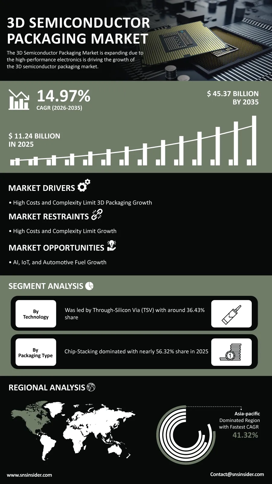
The global 3D Semiconductor Packaging Market is expected to witness robust growth over the next decade as demand for high-performance computing, artificial intelligence, and advanced electronic devices continues to accelerate. According to a recent study by SNS Insider, the global 3D Semiconductor Packaging Market size valued at USD 11.24 billion in 2025, is anticipated to grow to USD 45.37 billion by 2035, registering a CAGR of 14.97% over the 2026–2035 forecast period.
The fast pace at which semiconductor architecture technology has developed means that there is need to consider using packaging techniques that improve performance by increasing computing capabilities, energy efficiency, and functionalities in smaller devices. As semiconductor companies struggle to deal with the limitations posed by current scaling technology methods, 3D packaging technology becomes an essential way of improving performance.
The use of artificial intelligence (AI) accelerators, cloud systems, high-performance computing systems, connectivity solutions, and the Internet of Things (IoT) has increased significantly, leading to the increased demand for semiconductor packaging technologies. Consistent investment in advanced semiconductor packaging technology leads to higher bandwidths, reduced energy consumption, and improved heat dissipation.
To Get Detailed Insights on the 3D Semiconductor Packaging Market – Request a Sample Report
Advanced Chip Integration Creates New Growth Opportunities
Currently, there is a growing trend in the semiconductor industry where multiple chiplets can be integrated in a more efficient manner using heterogeneous integration that allows the combination of many different types of chiplets into an efficient packaging format.
A greater emphasis on advanced packaging technologies, such as TSV, FOWLP, and SiP, which are attracting increasing investments by many players in the market, are providing business opportunities for semiconductor manufacturers, OSATs, and equipment vendors.
Collaborations between the fabless companies, foundries, and OSATs are also contributing towards the reduction of development times as well as provision of advanced packaging technologies for AI, automotive, telecom, and data center applications.
Key Market Insights Highlight Shifting Demand Patterns
By technology, Through-Silicon Via (TSV) accounted for approximately 36.43% of global market revenue in 2025 owing to its ability to deliver high-density vertical integration and superior device performance. Fan-Out Wafer Level Packaging (FOWLP) is projected to register the fastest growth, expanding at a CAGR of 15.55% through 2035 as demand rises for compact, high-performance semiconductor solutions.
Based on packaging type, chip-stacking held nearly 56.32% of market revenue in 2025 due to its widespread adoption in advanced processors and memory devices. System-in-Package (SiP) is forecast to witness the fastest growth at a CAGR of 15.58%, driven by increasing integration requirements across consumer electronics, automotive systems, and industrial devices.
By application, the automotive segment generated approximately 38.43% of market revenue in 2025 as electric vehicles, ADAS, and connected mobility platforms require increasingly sophisticated semiconductor solutions. Healthcare is projected to emerge as the fastest-growing application segment, expanding at a CAGR of 15.64% as demand grows for compact medical electronics, wearable monitoring devices, and advanced diagnostic equipment.
By end user, the automotive industry held around 38.67% of market revenue in 2025. Meanwhile, healthcare is expected to record the fastest growth through 2035 as advanced packaging technologies enable miniaturized, energy-efficient semiconductor devices for next-generation medical applications.
AI and High-Performance Computing Continue to Drive Innovation
The increase in computational demands in areas like artificial intelligence, machine learning, cloud computing, and edge computing is changing the approach to packaging semiconductors around the world. The new packaging techniques will result in higher memory bandwidth, increased interconnect speed, and higher efficiency in terms of energy consumption.
The area of automotive electronics is also becoming one of the key areas of growth due to the needs to have reliable semiconductor packaging that can withstand challenging conditions of operation in areas like autonomous driving systems, electric vehicles, and intelligent car platforms.
Asia Pacific Dominates with 41.32% Market Share; North America Records 15.75% CAGR Through 2035
In 2025, Asia Pacific will generate 41.32% of the total market revenues, owing to its extensive semiconductor manufacturing base, active government initiatives, and rising demand from electronics, telecommunication, and automotive sectors. North America is forecasted to witness the highest CAGR during the forecast period of 2025 to 2035, which stands at 15.75%.
This will be attributed to an increase in AI infrastructure spending, investments in high-performance computing, and increased manufacturing of advanced semiconductor chips. The collaboration between the leaders in designing, manufacturing, and packaging of semiconductors keeps getting better day by day.
Industry Participants Focus on Next-Generation Packaging Technologies
The competitive landscape remains highly dynamic as semiconductor companies continue investing in heterogeneous integration, chiplet architectures, advanced interconnect technologies, and high-density packaging platforms. Manufacturers are prioritizing greater performance, scalability, thermal management, and manufacturing efficiency to address the evolving requirements of AI, cloud computing, automotive electronics, and next-generation communication systems.
Key companies operating in the global 3D Semiconductor Packaging Market include Intel Corporation, Samsung Electronics Co., Ltd., Taiwan Semiconductor Manufacturing Company Limited (TSMC), Advanced Micro Devices, Inc. (AMD), Broadcom Inc., Qualcomm Incorporated, Texas Instruments Incorporated, ASE Technology Holding Co., Ltd., Amkor Technology, Inc., STMicroelectronics N.V., NXP Semiconductors N.V., Infineon Technologies AG, Micron Technology, Inc., SK Hynix Inc., Toshiba Corporation, Renesas Electronics Corporation, MediaTek Inc., ON Semiconductor Corporation, Lam Research Corporation, and Applied Materials, Inc.
An SNS Insider analyst Sushant Kadam commented, “The growing adoption of AI workloads, high-performance computing, and advanced automotive electronics is accelerating demand for innovative semiconductor packaging solutions. Companies investing in next-generation integration technologies, manufacturing scalability, and packaging efficiency will be well positioned to capitalize on the industry's long-term growth trajectory.”
About the Author

Get in touch