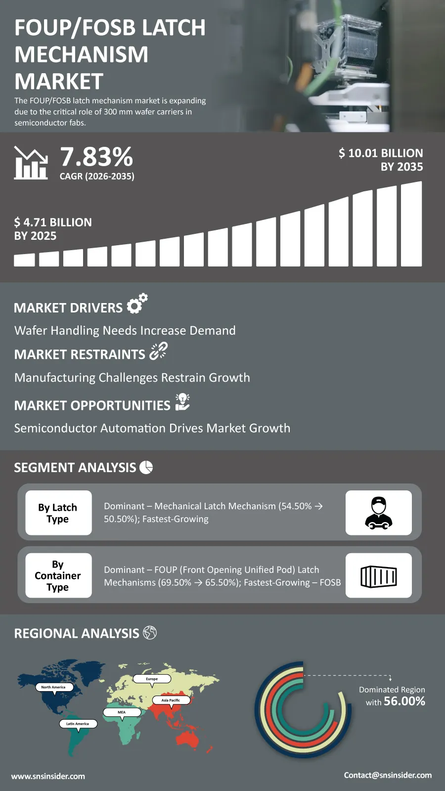
The global FOUP/FOSB Latch Mechanism Market is poised for sustained growth as semiconductor manufacturers continue expanding wafer fabrication capacity and investing in highly automated production environments. According to a recent study by SNS Insider, the global FOUP/FOSB Latch Mechanism Market size valued at USD 4.71 billion in 2025, is anticipated to grow to USD 10.01 billion by 2035, registering a CAGR of 7.83% over the 2026–2035 forecast period.
With advancements in semiconductor manufacturing technology to small process nodes and increased production scale, the importance of contamination-free wafer transportation has been recognized. Latch designs for FOUPs and FOSBs have a critical function in securing clean and precise movement of wafers during transportation through the fabrication plants, which are automated.
The growing trend among manufacturers is to design robust, precisely engineered latch mechanisms for their ability to operate continuously in automated fabrication plants. Increased durability, anti-electrostatic features, and compatibility with automated material handling systems are improving the significance of latch mechanisms in modern semiconductor fabrication.
To Get Detailed Insights on the FOUP/FOSB Latch Mechanism Market – Request a Sample Report
Semiconductor Automation Continues to Drive Market Expansion
With increased global investment in semiconductors, as governments and semiconductor producers ramp up domestic manufacturing capabilities to cope with rising needs in the fields of artificial intelligence, automotive, data centers, consumer devices, and industry, there is an increased need for wafer-handling tools that can facilitate consistent manufacturing operations.
The continued drive towards automation is one of the key market drivers, as the semiconductor fabs make use of advanced material handling equipment, equipment front-end module (EFEMs), and robotic transport systems. The high-quality latches ensure precise positioning of the carriers, minimize contamination hazards, and enhance production efficiency.
There has also been consistent innovations in engineering materials, manufacturing technology, and contamination prevention techniques, which enable the semiconductor producers to manufacture more durable products.
Key Market Insights Highlight Shifting Demand Patterns
In terms of the latch mechanism type, mechanical latch mechanisms will account for 54.50% of revenue share in the global market in 2025 based on their reliability, ease of operation, and wide implementation at semiconductor fabrication plants. Spring-loaded latches are expected to demonstrate the highest rate of growth up to 2035 driven by the increasing demand for high-precision wafer handling automation.
Depending on the type of container, FOUP latch mechanisms will generate 69.50% of the market revenue in 2025 due to wide adoption in the completely automated 300 mm fabs. Latch mechanisms for FOSB will exhibit the fastest growth rate due to the increased implementation of automated transportation of wafers at advanced packaging and wafer logistics facilities.
In terms of wafer size compatibility, the 300 mm segment will have the largest share – 64.50% in 2025 – due to the dominance of this wafer size in semiconductor manufacturing. The wafers larger than 300 mm will demonstrate the highest growth rate up to 2035 due to the increased investments in new semiconductor fabrication technologies.
Based on end-user application, semiconductor fabrication plants will hold 59.40% of market revenue in 2025 due to the steady investments into the growth of wafer production and automation at fabs. Semiconductor packaging and testing facilities are expected to become the fastest growing application segment.
Precision Engineering Becomes Central to Next-Generation Semiconductor Manufacturing
In line with the increasing sophistication of semiconductor fabrication technology, it is becoming necessary to design wafer-handling equipment that provides extremely high precision in clean room conditions. The manufacturers have come up with latch mechanisms which are more durable and have tighter mechanical tolerances, better ESD resistance, and increased compatibility with automated robotic platforms.
The increasing trend of intelligent factories is prompting the introduction of intelligent wafer handling equipment which can support predictive maintenance, live monitoring, and increased efficiencies of production. Such innovations would lead to increased demand for FOUP and FOSB latches.
Asia Pacific Dominates with a 56.00% Revenue Share in 2025 and a 9.27% CAGR
In 2025, Asia Pacific contributed with 56.00% toward the global market share revenue. The region is projected to remain dominant and hold the highest market share growth in addition to being the fastest growing region through 2035, growing at a CAGR of 9.27%. Large investments in semiconductor fabs in countries like China, Taiwan, South Korea, and Japan will keep up Asia-Pacific's lead in wafer processing technology.
North America is projected to continue holding its significant position in the market with continuous semiconductor investments that will be backed by domestic manufacturing investments and fabs construction in the region. Europe will continue experiencing steady growth as manufacturers will make more investments in high-end semiconductor manufacturing technologies.
As countries strengthen semiconductor supply chain resilience and expand domestic chip manufacturing capacity, demand for contamination-free wafer carrier technologies is expected to rise steadily across global markets.
Industry Participants Focus on Advanced Automation and Product Innovation
The competition is still very technology-oriented due to continuing investments by manufacturers in areas, such as precision engineering, automation, contamination control, and new wafer-handling technology. The reliability and seamless incorporation of the product into automated semiconductor manufacturing facilities are key issues for companies trying to be competitive.
Key companies operating in the global FOUP/FOSB Latch Mechanism Market include Entegris, Inc., MKS Instruments, Inc., Brooks Automation, Inc., Tokyo Electron Limited (TEL), KLA Corporation, Applied Materials, Inc., ASM Pacific Technology Limited, Hitachi High-Tech Corporation, Panasonic Corporation, Nikon Corporation, Canon Tokki Corporation, AMAT Automation Solutions, Ebara Corporation, Teradyne, Inc., SEMI Equipment Suppliers (Tier-1 consortium), Nissin Electric Co., Ltd., Advantest Corporation, Lam Research Corporation, Veeco Instruments Inc., and TSMC Automation Partners.
An SNS Insider analyst Sushant Kadam commented, “Rapid semiconductor capacity expansion, increasing factory automation, and rising demand for contamination-free wafer transport are creating strong growth opportunities for advanced FOUP and FOSB latch mechanism manufacturers. Companies focused on precision engineering, automation compatibility, and long-term product reliability will be well positioned to benefit from continued investments in next-generation semiconductor fabrication.”
About the Author

Get in touch