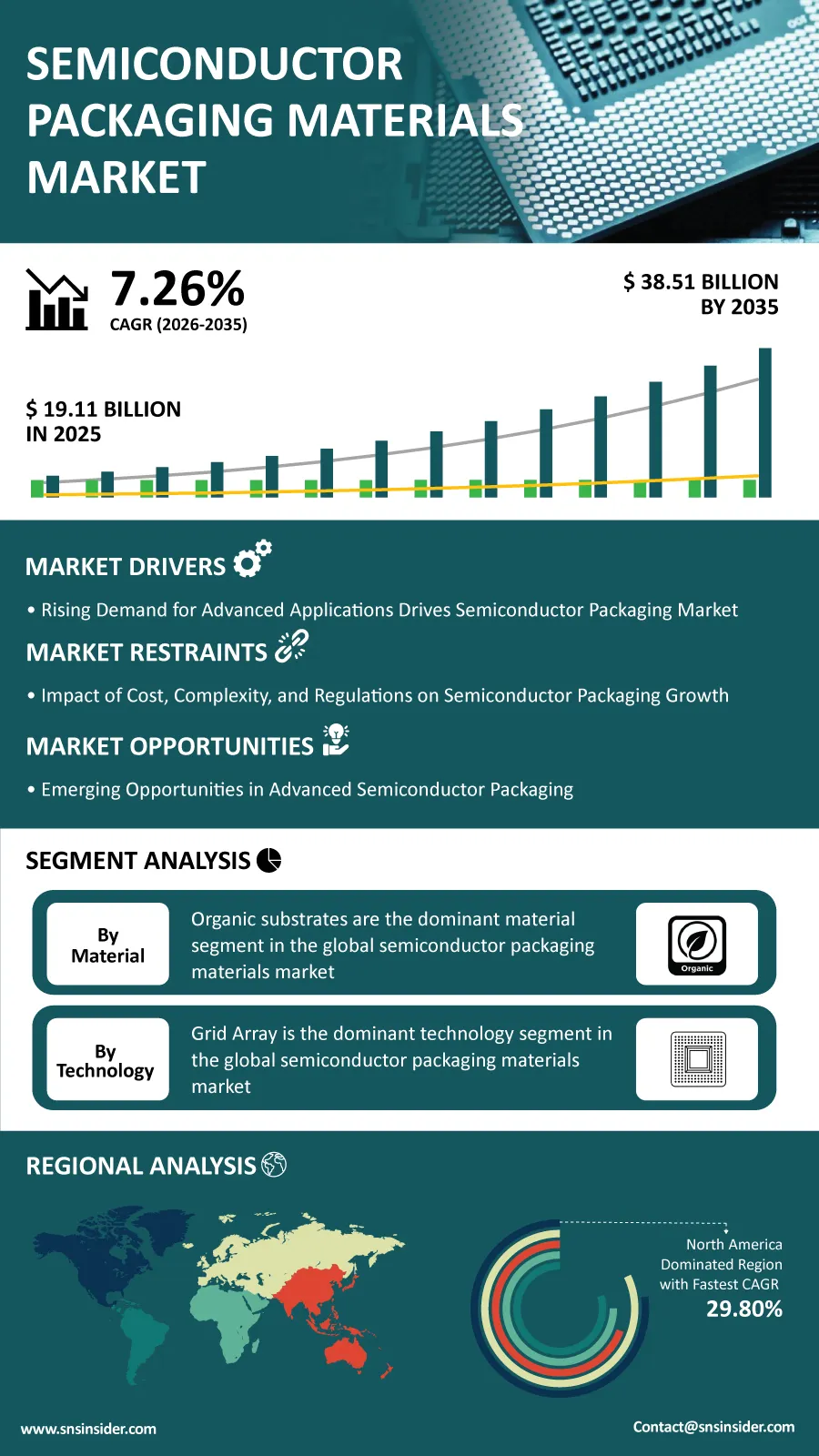
The global Semiconductor Packaging Materials Market is poised for sustained growth over the next decade due to growing investments made by semiconductor companies in advanced packaging solutions for next-generation computing, artificial intelligence, automotive electronics, and high-speed communications. According to a recent study by SNS Insider, the global Semiconductor Packaging Materials Market size valued at USD 19.11 billion in 2025, is anticipated to grow to USD 38.51 billion by 2035, registering a CAGR of 7.26% over the 2026–2035 forecast period.
With the growing development of semiconductor components with higher efficiency, speed, and reduced size, the use of packaging material is taking on an increasing significance. In order to achieve higher density while maintaining stability during work under difficult conditions, semiconductor industry producers are using advanced substrates, encapsulants, bonding techniques, and thermal materials.
The rapid growth in the development of AI systems, supercomputing, electric vehicles, 5G technology, and automation is pushing the need for advanced packaging materials that will be able to facilitate more complicated semiconductor design.
To Get Detailed Insights on the Semiconductor Packaging Materials Market – Request a Sample Report
Advanced Packaging Technologies Drive New Market Opportunities
A significant change is being witnessed in the semiconductor industry with the adoption of heterogeneous integration, 3D semiconductor packaging, chiplets architecture, and high density interconnect technology. The aforementioned developments are generating considerable demand for packaging materials that can increase electrical performance, reduce heat generation, and increase device reliability.
Investments in next generation adhesives, ceramic package, organic substrate, underfill material, and thermal interface material are continuously being made by manufacturers to satisfy industry demands. Further research on copper-to-copper bonding, interposer, and wafer level packaging technologies is likely to provide new business prospects for the market players during the forecast period.
Growing government support for domestic semiconductor manufacturing and resilient supply chains is encouraging additional investments in advanced packaging ecosystems across major semiconductor-producing regions.
Key Market Insights Highlight Shifting Demand Patterns
By material, organic substrate-based semiconductor packaging is expected to generate 44.70% of global market revenues in 2025 on the back of being cost-effective, flexible, and extensively used in consumer electronics and communication devices. Ceramic-based semiconductor packaging is predicted to witness the fastest growth until 2035 driven by growing usage in automotive electronics, aerospace applications, and HPC (high-performance computing).
Based on technology, Grid Array semiconductor packaging is estimated to generate 25.20% of global revenue in 2025 on the back of its high density and reliability. Other packaging technologies segment is expected to exhibit the fastest growth rate as the demand for increasingly sophisticated packaging increases in the next generation of chips.
In terms of end use, consumer electronics segment is expected to contribute 34.50% of global revenues in 2025 thanks to high manufacturing volumes of smartphones, laptops, wearable, and other smart devices. Automotive applications segment is expected to generate the fastest growth until 2035 owing to the growing demand for semiconductor packaging in electric vehicles, advanced driver assistance systems, and autonomous driving technologies.
By application, thermal management materials are expected to generate 25.30% of revenues in 2025 due to its importance in ensuring chip performance and life span. Adhesives & Underfill will generate the fastest growth among application type segments due to increasing usage of AI processors, packaging platforms, and high-density semiconductor assemblies.
Innovation in Materials Science Strengthens Semiconductor Performance
Innovations in material technology have begun to take center stage in determining the future of semiconductor packaging. The companies are investing in developing materials with better conductivity, electrical insulating properties, mechanical strength, and reliability while allowing further miniaturization of the components.
The developments in materials used in advanced packaging allow for increased integration of the chip, reduced energy use, and enhanced performance of devices in data centers, telecommunication networks, automobiles, and health care equipment. As the complexity of the semiconductor increases, material providers will begin to play an increasingly important role in semiconductor technology development.
North America Captured 29.8% Market Share in 2025, While Asia Pacific Emerges as the Fastest-Growing Region Through 2035
North America held around 29.80% share in the global market revenues by 2025, with substantial investments in semiconductor manufacturing, research, and increased use of AI and high-performance computing. Various government incentives that promote domestic production of semiconductors make the region highly competitive.
Asia Pacific is expected to hold its position as the fastest-growing regional market till 2035, with a large amount of semiconductor manufacturing capabilities available in China, Japan, South Korea, and Taiwan. Increasing electronics manufacturing and rising need for advanced semiconductor manufacturing will further solidify the region's position.
As countries continue strengthening semiconductor supply chains and expanding domestic production capabilities, demand for high-performance packaging materials is anticipated to accelerate worldwide.
Industry Participants Focus on Advanced Material Innovation
The competitive landscape continues to evolve as leading companies invest in next-generation packaging materials, advanced substrate technologies, thermal management solutions, and environmentally sustainable manufacturing processes. Strategic collaborations, capacity expansions, and continuous product innovation remain key priorities as manufacturers seek to address the growing performance requirements of advanced semiconductor devices.
Key companies operating in the global Semiconductor Packaging Materials Market include DuPont, BASF SE, Henkel AG & Co. KGaA, Hitachi Ltd., Kyocera Corporation, LG Innotek, Shin-Etsu Chemical Co., Ltd., Sumitomo Chemical, Sumitomo Bakelite, Toray Industries, Tanaka Kikinzoku Group, Toppan Printing Co., Ltd., Nippon Micrometal Corporation, Alpha Advanced Materials, Heraeus Electronics, Indium Corporation, ChipMOS Technologies Inc., Powertech Technology Inc., Unimicron Technology Corporation, Samsung Electronics Co., Ltd., and Texas Instruments Inc.
An SNS Insider analyst Sushant Kadam commented, “Rapid advances in AI, automotive electronics, and high-performance computing are significantly increasing the demand for innovative semiconductor packaging materials. Companies that prioritize advanced material engineering, thermal performance, and next-generation packaging technologies will be well positioned to capitalize on long-term opportunities across the evolving global semiconductor ecosystem.”
About the Author

Get in touch