Chemical Mechanical Planarization Market Size Analysis:
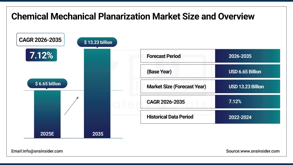
The Chemical Mechanical Planarization Market size was valued at USD 6.65 billion in 2025 and is expected to reach USD 13.23 billion by 2035, growing at a CAGR of 7.12% from 2026-2035.
This growth is driven by the increasing complexity of semiconductor manufacturing, that requires CMP techniques of higher sophistication to tackle the finer nodes and the 3D ICs as well. More improvement in pad technology is required given the rising complexity of CMP slurries.
Market Size and Growth Projection:
-
Market Size in 2024: USD 6.65 Billion
-
Market Size by 2032: USD 13.23 Billion
-
CAGR: 7.12% from 2026 to 2035
-
Base Year: 2025
-
Forecast Period: 2026–2035
-
Historical Data: 2022–2024
To Get more information on Chemical Mechanical Planarization Market - Request Free Sample Report
Chemical Mechanical Planarization Market Trends Highlights:
-
Growing demand of new semiconductor devices is driving Chemical Mechanical Planarization(CMP) market.
-
Market growth is propelled by growth in CMP adoption in logic, memory, and foundry applications.
-
Increased yield and performance from technological advancements in CMP slurries, pads, and consumables.
-
Surging IoT, 5G, cloud computing growth to steer semiconductor wafer fabrication, backend to CMP directly.
-
Advanced node chips (7nm and below) has high demands for planarization before the patterning process, which leads to further expansion of the production capacity of planarization processes.
-
The transition toward 3D structures and heterogeneous integration is widening CMP applications.
-
Partnerships amongst semiconductor fabs, materials suppliers and equipment manufacturers are allowing this innovation and process efficiencies.
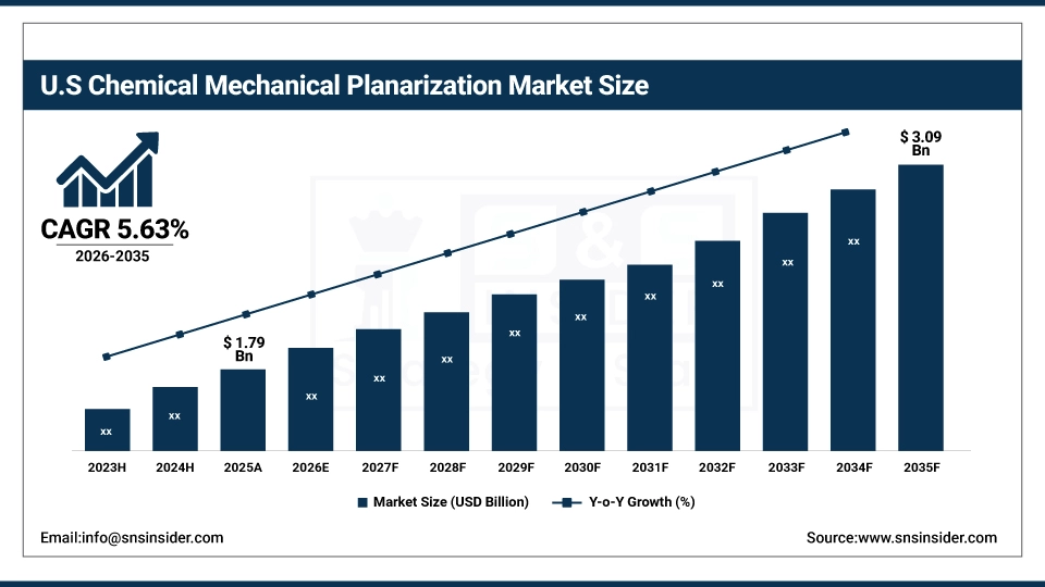
U.S. Chemical Mechanical Planarization Market Size Outlook
U.S. Chemical Mechanical Planarization Market was valued at USD 1.79 billion in 2025 and is expected to reach USD 3.09 billion by 2035, growing at a CAGR of 5.63% from 2025-2032, as the demand for continued innovation in technological development and investments in semiconductor manufacturing continue to grow. The increasing use of 5G technologies and High-Performance Computing (HPC) also boost the market growth as this requires CMP processes which are tailored for high-density and high-performance semiconductor devices.
Chemical Mechanical Planarization Market Growth Drivers:
-
Advancements and Investments Driving the Evolution of Chemical Mechanical Planarization in Semiconductor Manufacturing
The semiconductor industry is currently undergoing a massive transformation as a result of high investments and new technologies. Especially given this shift signalled by the U.S. Department of Commerce announcement in mid-April 2024 to award USD 6.6 billion in new, direct funding to TSMC as an incentive to expand its Arizona facilities, underlining the b force under which true domestic semiconductor manufacturing must consider moving to. Also, initiatives from the whole world such as the European Chips Act also showed the industry initiative when it approved EUR 43 billion to increase semiconductor fabrication in Europe. Introduction As semiconductor manufacturing slowly but steadily marches into smaller nodes, e.g., 5nm, 3nm etc., the demand for CMP [40] processes will exponentially grow due to the requirement of planarization of multi-sequence high-k layers, which doubles such as in 3D ICs [19], and also because of the devices including memory chip and logic devices which need stable planar surfaces without defect. There is also a growing demand due to the fast-paced 5G boom and more data center infrastructure, fuelling the need for high-performance components. For instance, Ericsson predicts that, by 2028, there will be 5 billion 5G subscriptions globally, and by March 2024, the U.S. had the most data centers of any country with 5,381. This influx is reshaping the landscape of semiconductor manufacturing processes. New plants, such as this one for ultra-clean CMP slurries from FUJIFILM in Kumamoto, as well as Dongjin Semichem's CMP slurry supply to SK Hynix, emphasize the industry is evolving new advanced CMP solutions to keep pace with the increasing complexity of design and packaging.
Chemical Mechanical Planarization Market Restraints:
-
Navigating the Complexities of CMP Integration in Advanced Semiconductor Manufacturing
Integrating Chemical Mechanical Planarization (CMP) processes into semiconductor manufacturing workflows is a complex and difficult. CMP must be integrated with other key processes such as photolithography and etching, which requires exact synchronization with generation of smooth, defect-free surfaces and maintaining good yields. To orchestrate all of this is no small feat, necessitating high end technology and masterful skill. In current systems, CMP integration is also a challenge as the variety of device types (and hence, the variety of common CMP types) increases alongside the trend of pushing semiconductor devices to the 5nm and 3nm (and smaller) nodes. Add to this the requirement with highly specialized kit and trained crew, it makes it an incredibly difficult production for smaller manufacturers, or regions where the imperative infrastructure is not well developed. This complexity can result in the CMP technology being adopted downstream of other processes as the manufacturers are still trying to optimize their production and implement necessary alterations to improve their manufacturing processes. These emerging semiconductor technologies that are in a constant state of evolution correspond to new requirements for CMP integration.
Chemical Mechanical Planarization Market Opportunities:
-
Driving the Miniaturization of Electronics: The Role of CMP Slurries and Pads in Advancing Technology
The ongoing trend toward miniaturization in electronic products is significantly driving the demand for Chemical Mechanical Planarization (CMP) slurries and pads. With the shrinking dynamics of portable electronics such as smartphones, laptops, wearables, and electric vehicles, portable electronics have become now a need, not a necessity, and the demand for smaller and high-efficiency semiconductor chips is set to grow. This allows for faster frequencies and clock rates; combining into an overall increase in speed and performance due to the miniaturization of devices which in return further reduces size enabling increased densities. Automotive again, but this time is even more decisive with the rise of ADAS – advanced driver-assistance systems – infotainment systems and all related to the development of autonomous vehicles, all needs tiny, powerful performance Chips. With 101.4 million vehicles estimated to be sold worldwide in 2030, miniaturized semiconductors will be indispensable. Trending towards miniaturization is also aided by innovations, such as graphene, that enable smaller electronic components that also consume less energy.
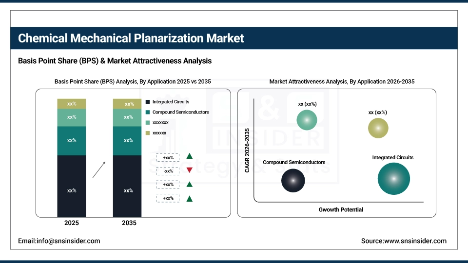
Chemical Mechanical Planarization Industry Segmentation Analysis:
By Application, Integrated Circuits (ICs) lead the CMP market, whereas compound semiconductors are the fastest-growing segment.
The Integrated Circuits (ICs) segment dominated the market with the largest revenue share of around 49% in 2025. This is mainly fuelled by the growth in demand for sophisticated ICS across numerous applications such as consumer electronics, telecommunications, automotive and industrial domains. Production Of Integrated Circuits continues to evolve as the need for larger and stronger semiconductor devices increases, driven by the developments of 5G networks, artificial intelligence (AI), and high-performance computing (HPC). At the same time, the advancement of modern ICs, including memory chips, logic devices, and 3D ICs, leads to the need for more accurately performed CMP process to provide a planar wafer surface and high yield. Given the prolific nature of the need for IC no matter the industry, this segment has and will continue to lead in CMP market.
The Compound Semiconductors segment is the fastest-growing segment in the CMP market during the forecast period from 2026 to 2035. Fueled by the growing need for compound semiconductors, including gallium nitride (GaN) and silicon carbide (SiC), which are essential for high-performance applications like 5G networks, electric vehicles (EVs), and power electronics, this growth is accelerating. The development of compound semiconductor that combines superior effisiancy, high thermal conductivity and higher switching speeds paves the way for their use in advanced technology. The Market Scene CMP processes are being applied to compound semiconductors 3, especially in energy-efficient power devices 5 and high-frequency communication systems 7, which indicate that there is aneed forspecialized processes to provide high-quality surface planarization for those applications, thus fostering the growth of market in forecast period
By Equipment, CMP equipment dominates the Chemical Mechanical Planarization (CMP) market, while CMP consumables are the fastest-growing segment.
The CMP equipment segment dominated the market with the largest revenue share of around 60% in 2025. This dominance is driven by the increasing complexity of semiconductor manufacturing processes, where CMP equipment plays a crucial role in ensuring smooth and defect-free surfaces for advanced semiconductor devices. As semiconductor nodes continue to shrink, the demand for sophisticated CMP equipment, such as polishing machines, planarization tools, and metrology equipment, is rising. Rapid growth of high-performance computing (HPC), 5G technology, and advanced packaging gives rise to need of state-of-the-art CMP equipment putting significant share of CMP market. Due to the continuous improvement in semiconductor technology, CMP which is a high end process segmenting equipment will remain to enjoy a steady growth in upcoming years.
The CMP consumables segment is the fastest-growing segment in the market during the forecast period from 2026 to 2035. This growth is driven by increase in demand for CMP slurries and polishing pads key materials in the planarization process used in semiconductor manufacturing. As semiconductor devices become ever smaller, more complex, and more tightly controlled in their chemistry and performance specifications, we expect this new commercial grade silicon product to fill an expanding niche for application specific consumables. New formulations of CMP slurries and new pad materials are essential to enabling next generation semiconductor nodes and packaging technology. In addition, rising 5G technology, increasing adoption of AI, and automotive electronics are also contributing to the increase in the CMP consumables segment during the forecast period.
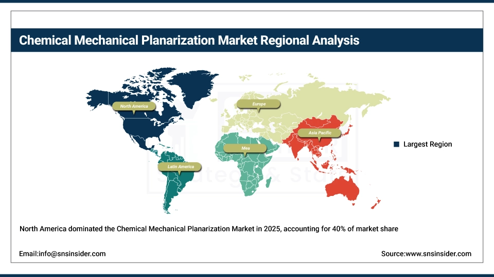
Chemical Mechanical Planarization Market Regional Analysis
North America Chemical Mechanical Planarization Market Insights
The North America region dominated the CMP market with the largest revenue share of approximately 40% in 2025. This dominance is owing to the large number of semiconductor industry manufacturers, technology companies and research centers across the region. Recently, there have been significant developments, such as continued fab investments in the US, with government support (e.g., the CHIPS Act), which can be considered make-or-break for fab in the US. The widespread deployment of 5G technology, along with artificial intelligence (AI) and high-performance computing (HPC), are all contributing to increasing semiconductor device complexity and are resultant in further continuing to push CMP to ever ironically extreme heights. Furthermore, the data center and automotive sectors, particularly electric vehicles, are driving the region's sustained CMP market dominance. Its market leader position is assured by the advanced technology and tremendous investments by R&D in North America.
Get Customized Report as per Your Business Requirement - Enquiry Now
Asia Pacific Chemical Mechanical Planarization Market Insights:
Asia Pacific is the fastest-growing region in the Chemical Mechanical Planarization (CMP) market, projected to register a CAGR of 10.85% from 2026 to 2035. The growth is primarily due to rapid expansion of semiconductor manufacturing in countries such as China, Taiwan, South Korea and Japan due to strong government support, growing demand for sophisticated consumer electronics, as well as a growing trend toward investing in AI, 5G and automotive chips. With the strong presence of fabs, major foundries, as well as the adoption of advanced packaging technologies in the region, North America is likely to continue to be a major production and innovation hub in CMP on a global scale.
Europe Chemical Mechanical Planarization Market Insights:
Europe in the Chemical Mechanical Planarization (CMP) market is experiencing steady growth owing to continuous advancements in semiconductor services, booming precision engineering, and continuous demand for consumer electronics. Important ones include Lapmaster Wolters GmbH, BASF SE, and Saint-Gobain for their CMP equipment, slurries and polishing materials. Europe offers CMP market a unique position, which is backed with strong R&D biodiversity, support from government for microelectronics and collaborations with global giants semiconductor companies.
Middle East & Africa and Latin America Chemical Mechanical Planarization Market Insights:
Middle East & Africa and Latin America in the Chemical Mechanical Planarization (CMP) market are witnessing slow growth, due to the rising demand from semiconductors, electronics, and infrastructure development in the regions. Although these regions primarily depend on the imports of CMP equipment and materials from the global suppliers, the projected forecast period will witness strong lift of the local capabilities with rising investments into the technological hubs, government initiatives and collaborations with the international semiconductor companies that will further expand the CMP market in these region.
Chemical Mechanical Planarization Market Competitive Landscape:
FUJIFILM Corporation
FUJIFILM Corporation, founded in 1934, is a diversified multinational company engaged in healthcare, materials, imaging, and document solutions. Leveraging decades of expertise in advanced materials science, FUJIFILM provides innovative semiconductor materials, including CMP slurries, photoresists, and photolithography products. The company plays a key role in supporting the global semiconductor supply chain, particularly in high-growth sectors such as automotive and industrial electronics, by delivering reliable, scalable, and high-performance solutions.
- February 06, 2025: FUJIFILM Corporation announced an investment of approximately 4 billion yen (USD 26.75 million) to expand its Belgium site in Zwijndrecht, Antwerp. It comprises new CMP slurries production centers, as well as upgrades on materials related to photolithography, aimed at addressing the continuously expanding automotive and industrial semiconductors market in Europe.
DuPont
DuPont, established in 1802, is a global leader in science, innovation, and materials technology. The company develops advanced solutions in electronics, transportation, construction, and healthcare, with a strong focus on semiconductor technologies. Its portfolio includes CMP pads, dielectric materials, and specialty polymers that power next-generation computing, AI, and 5G infrastructure. DuPont is committed to enabling high-performance, sustainable, and reliable technologies that accelerate advancements in data centers and digital transformation worldwide.
- October 30, 2024: DuPont recognized by Samsung Electronics in Innovation category for its pioneering CMP polishing pads, enabling Next-Gen semiconductor, AI, 5G and Data Center.
Chemical Mechanical Planarization Companies are:
-
Entegris Inc.
-
Ebara Corporation
-
Lapmaster Wolters GmbH
-
DuPont De Nemours Inc.
-
Fujimi Incorporated
-
Resonac Holdings Corporation (Showa Denko Materials)
-
Okamoto Corporation
-
Fujifilm Corporation (Fujifilm Holdings Corporation)
-
Tokyo Seimitsu Co. Ltd (Accretech Create Corp.)
-
Cabot Microelectronics Corporation
-
Dow Inc.
-
Saint-Gobain
-
Momentive Performance Materials Inc.
-
Hitachi Chemical Company Ltd.
-
3M Company
-
JSR Corporation
-
Henkel AG & Co. KGaA
-
BASF SE
| Report Attributes | Details |
|---|---|
| Market Size in 2025 | USD 6.65 Billion |
| Market Size by 2035 | USD 13.23 Billion |
| CAGR | CAGR of 7.12% From 2026 to 2035 |
| Base Year | 2024 |
| Forecast Period | 2026-2035 |
| Historical Data | 2022-2024 |
| Report Scope & Coverage | Market Size, Segments Analysis, Competitive Landscape, Regional Analysis, DROC & SWOT Analysis, Forecast Outlook |
| Key Segments | • By Equipment (CMP Equipment, CMP Consumable) • By Application (Compound Semiconductors, Integrated Circuits, Mems and Nems, Others) |
| Regional Analysis/Coverage | North America (US, Canada), Europe (Germany, UK, France, Italy, Spain, Russia, Poland, Rest of Europe), Asia Pacific (China, India, Japan, South Korea, Australia, ASEAN Countries, Rest of Asia Pacific), Middle East & Africa (UAE, Saudi Arabia, Qatar, South Africa, Rest of Middle East & Africa), Latin America (Brazil, Argentina, Mexico, Colombia, Rest of Latin America). |
| Company Profiles | Applied Materials Inc. (USA), Entegris Inc. (USA), Ebara Corporation (Japan), Lapmaster Wolters GmbH (Germany), DuPont De Nemours Inc. (USA), Fujimi Incorporated (Japan), Revasum Inc. (USA), Resonac Holdings Corporation (Showa Denko Materials) (Japan), Okamoto Corporation (Japan), Fujifilm Corporation (Fujifilm Holdings Corporation) (Japan), and Tokyo Seimitsu Co. Ltd (Accretech Create Corp.) (Japan) are key players in the CMP market. |
Frequently Asked Questions
Ans: North America dominated the CMP market in 2025, accounting for the largest revenue share of approximately 40%.
Ans: By equipment type, CMP equipment dominated the market, while in application, Integrated Circuits (ICs) held the leading share during the projected years.
Ans: The primary growth factor is the rising demand for advanced semiconductor devices, supported by IoT, AI, 5G, and cloud computing, along with technological advancements in CMP slurries, pads, and consumables.
Ans: The Chemical Mechanical Planarization Market size was valued at USD 6.65 billion in 2025.
Ans: The Chemical Mechanical Planarization (CMP) Market is projected to grow at a CAGR of 7.12% during the forecast period from 2026 to 2035.
Get in Touch
