Hybrid Bonding Technology Market Report Scope & Overview:
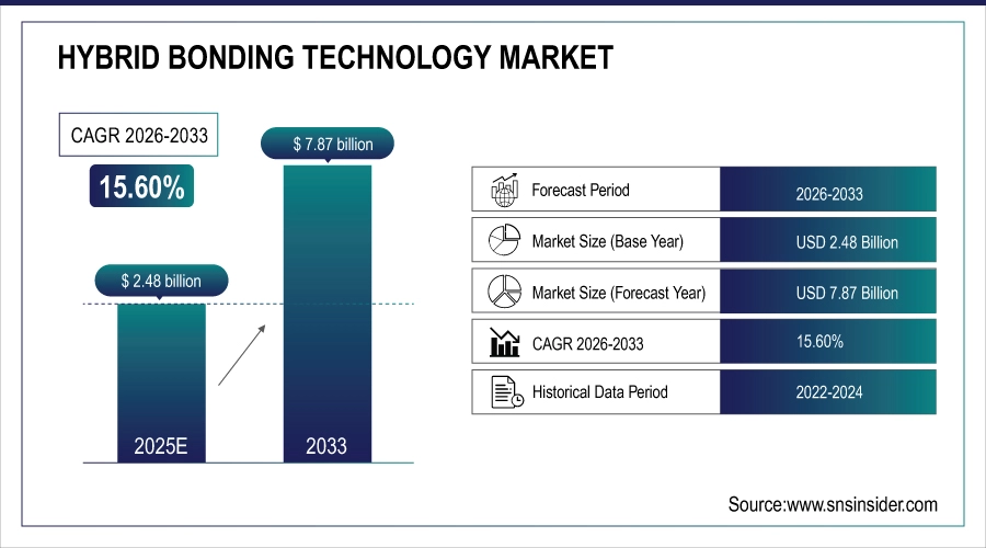
The Hybrid Bonding Technology Market size was valued at USD 2.48 Billion in 2025E and is projected to reach USD 7.87 Billion by 2033, growing at a CAGR of 15.60% during 2026-2033.
The Hybrid Bonding Technology Market is growing due to rising demand for advanced semiconductor packaging, driven by AI, high-performance computing, and data-center workloads. Increasing adoption of 3D ICs, chiplet architectures, and high-bandwidth memory (HBM) is accelerating the need for fine-pitch, high-density interconnects. Hybrid bonding enables lower power consumption, higher performance, and improved signal integrity compared to traditional packaging. Additionally, growth in CMOS image sensors, automotive electronics, and miniaturized devices further supports market expansion.
Hybrid Bonding Technology Market Size and Forecast:
-
Market Size in 2025E USD 2.48 Billion
-
Market Size by 2033 USD 7.87 Billion
-
CAGR of 15.60% From 2026 to 2033
-
Base Year 2025E
-
Forecast Period 2026-2033
-
Historical Data 2021-2024
To Get more information on Hybrid Bonding Technology Market - Request Free Sample Report
Key Hybrid Bonding Technology Market Trends
-
Increasing adoption of advanced semiconductor packaging including 2.5D/3D integration to overcome scaling limitations.
-
Rising demand for high-bandwidth memory (HBM), 3D ICs, and chiplet architectures driven by AI, HPC, and data-center workloads.
-
Expansion of heterogeneous integration, combining logic, memory, sensors, and analog components into single packages.
-
Growing use of hybrid bonding in CMOS image sensors, automotive electronics, and edge computing applications.
-
Government support and investments in domestic semiconductor manufacturing and next-generation processes below 5 nm.
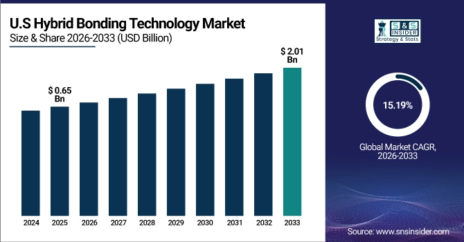
The U.S. Hybrid Bonding Technology Market size was valued at USD 0.65 Billion in 2025E and is projected to reach USD 2.01 Billion by 2033, growing at a CAGR of 15.19% during 2026-2033. The U.S. Hybrid Bonding Technology Market is growing due to strong investments in advanced semiconductor manufacturing, rising demand for AI, HPC, and data centers, rapid adoption of 3D IC and chiplet architectures, and government support for domestic chip production and advanced packaging innovation.
Hybrid Bonding Technology Market Growth Drivers:
-
Hybrid Bonding Market Growth Fueled by AI HPC High-Bandwidth Memory and Advanced Semiconductor Packaging
The global Hybrid Bonding Technology Market is primarily driven by the rapid shift toward advanced semiconductor packaging to overcome the physical and economic limits of traditional scaling. The surge in artificial intelligence (AI), high-performance computing (HPC), and data-center workloads has increased demand for high-bandwidth memory (HBM), 3D ICs, and chiplet-based architectures, where hybrid bonding enables ultra-fine interconnect density, lower latency, and improved power efficiency. Additionally, strong growth in CMOS image sensors for smartphones, automotive ADAS, and industrial vision systems is accelerating adoption. Continuous investments by foundries and OSATs in 2.5D/3D integration, along with advancements in copper-to-copper bonding and alignment accuracy, are further supporting market expansion.
Advanced packaging equipment makers like BE Semiconductor Industries (BESI) reported an 8.2% increase in order bookings in Q1 2025, driven by strong demand for hybrid bonding tools from memory and logic chip producers for AI-related applications
Hybrid Bonding Technology Market Restraints:
-
Hybrid Bonding Market Growth Constrained by Process Complexity Alignment Challenges and Limited Skilled Expertise
The Hybrid Bonding Technology Market faces restraints such as high process complexity, stringent requirements for ultra-clean surfaces and precise alignment, and yield sensitivity at advanced nodes. Limited availability of skilled expertise, challenges in scaling hybrid bonding for high-volume manufacturing, and integration issues with existing fabrication lines also slow adoption, particularly for smaller foundries and OSATs.
Hybrid Bonding Technology Market Opportunities:
-
Expanding Hybrid Bonding Adoption Unlocks Opportunities in AI Accelerators Automotive Electronics and Edge Computing
Significant opportunities exist in the expanding adoption of hybrid bonding for heterogeneous integration, combining logic, memory, sensors, and analog components into a single package. Emerging applications in AI accelerators, automotive electronics, and edge computing are expected to drive new revenue streams. Government initiatives supporting domestic semiconductor manufacturing in the U.S., Europe, and Asia are creating opportunities for equipment suppliers and technology providers. Moreover, the transition toward advanced node processes below 5 nm, increasing demand for chiplets, and growing use of hybrid bonding in MEMS and advanced sensors present long-term growth potential across global markets.
Independent analysis shows that hybrid bonding equipment can deliver ~18% higher throughput and 7–9% yield improvement in advanced packaging lines, directly translating into production efficiencies and stronger competitiveness for AI accelerator and memory manufacturers
Hybrid Bonding Technology Market Segment Analysis
-
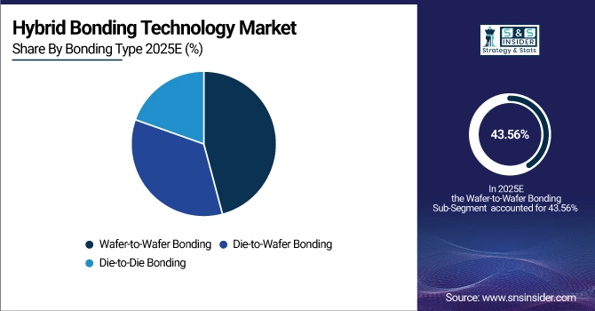
By Bonding Type, Wafer-to-Wafer Bonding dominated with 43.56% in 2025E, and Die-to-Die Bonding is expected to grow at the fastest CAGR of 16.12% from 2026 to 2033.
-
By Process / Material Interface, Copper-to-Copper (Cu-Cu) Hybrid Bonding dominated with 49.53% in 2025E, and it is expected to grow at the fastest CAGR of 15.94% from 2026 to 2033.
-
By Application, Logic & Memory Devices (HBM, DRAM, NAND) dominated with 43.31% in 2025E, and Advanced Packaging (2.5D/3D ICs) is expected to grow at the fastest CAGR of 16.16% from 2026 to 2033.
-
By End-User Industry, Semiconductor Foundries & OSATs dominated with 39.65% in 2025E, and Data Centers, AI & High-Performance Computing is expected to grow at the fastest CAGR of 16.39% from 2026 to 2033.
By Bonding Type, Wafer-to-Wafer Bonding Dominates Hybrid Bonding Market While Die-to-Die Shows Fastest Growth Potential
By Bonding Type, Wafer-to-Wafer Bonding leads the market due to its efficiency in high-volume semiconductor manufacturing and wide adoption in memory and logic applications. Die-to-Die Bonding is expected to grow the fastest, driven by increasing demand for heterogeneous integration, high-performance 3D ICs, and advanced packaging solutions that enable miniaturization and improved performance in AI, data centers, and consumer electronics.
By Process / Material Interface, Copper-to-Copper Hybrid Bonding Leads Market Growth Driven by AI High Performance Computing and 3D ICs
By process and material interface, Copper-to-Copper (Cu-Cu) Hybrid Bonding leads the market due to its superior electrical performance and widespread use in high-density interconnects for memory and logic devices. It is expected to grow rapidly, driven by increasing demand for high-performance computing, AI applications, advanced 3D ICs, and next-generation semiconductor packaging solutions.
By Application, Logic and Memory Devices Dominate Hybrid Bonding Market While Advanced Packaging Shows Rapid Future Growth
By application, Logic & Memory Devices lead the market due to strong demand for high-bandwidth memory and advanced semiconductor solutions in AI, HPC, and data centers. Advanced Packaging (2.5D/3D ICs) is expected to grow rapidly, driven by the need for heterogeneous integration, chiplet architectures, and miniaturized, high-performance electronic devices.
By End-User Industry, Semiconductor Foundries Drive Hybrid Bonding Market Growth Fueled by AI and High-Performance Computing Demand
Semiconductor Foundries & OSATs lead the market due to their central role in manufacturing and integrating hybrid bonding technologies. Data Centers, AI, and High-Performance Computing are expected to grow rapidly, driven by increasing demand for high-performance, energy-efficient computing solutions and advanced memory integration in next-generation data-center architectures.
Hybrid Bonding Technology Market Regional Analysis
North America Hybrid Bonding Technology Market Insights
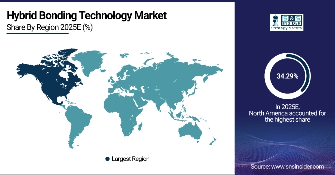
In 2025, North America holds a significant 34.29% share of the Hybrid Bonding Technology Market, driven by strong investments in advanced semiconductor manufacturing, AI, and high-performance computing applications. The region benefits from the presence of leading foundries, OSATs, and equipment suppliers, along with government initiatives supporting domestic chip production. Continuous adoption of 3D ICs, HBM integration, and chiplet-based architectures further reinforces North America’s leading position in this market.
Get Customized Report as per Your Business Requirement - Enquiry Now
U.S. Hybrid Bonding Technology Market Insights
In North America, the United States dominates the hybrid bonding market due to its advanced semiconductor ecosystem, leading foundries, OSATs, and strong investments in AI, HPC, and 3D IC technologies, driving widespread adoption of high-performance packaging solutions.
Europe Hybrid Bonding Technology Market Insights
In 2025, Europe accounts for 19.73% of the Hybrid Bonding Technology Market, supported by growing investments in semiconductor research, advanced packaging, and chiplet integration. The region benefits from government initiatives promoting domestic semiconductor manufacturing and innovation. Adoption of hybrid bonding in automotive electronics, AI applications, and industrial sensors, along with increasing collaborations between foundries and OSATs, is driving steady market growth across key European countries.
Germany Hybrid Bonding Technology Market Insights
In Europe, Germany dominates the hybrid bonding market due to its strong semiconductor manufacturing base, advanced automotive electronics sector, significant R&D investments, and collaborations between foundries and OSATs, supporting widespread adoption of hybrid bonding for AI, industrial, and automotive applications.
Asia Pacific Hybrid Bonding Technology Market Insights
In 2025, the Asia Pacific region dominates the Hybrid Bonding Technology Market with a 39.79% share, driven by the presence of leading semiconductor manufacturers in Taiwan, South Korea, and China. Strong adoption of 3D ICs, HBM integration, and chiplet architectures for AI, high-performance computing, and consumer electronics fuels market growth. The region is expected to register the fastest CAGR of 16.10% from 2026–2033, supported by continuous investments in advanced packaging, OSAT collaborations, and government initiatives promoting semiconductor innovation.
Taiwan Hybrid Bonding Technology Market Insights
In Asia Pacific, Taiwan dominates the hybrid bonding market due to its advanced semiconductor manufacturing ecosystem, leading foundries, strong adoption of 3D ICs and HBM integration, and strategic investments in AI, high-performance computing, and advanced packaging technologies.
Latin America (LATAM) and Middle East & Africa (MEA) Hybrid Bonding Technology Market Insights
In Latin America (LATAM) and Middle East & Africa (MEA), the Hybrid Bonding Technology Market remains relatively small but is gradually expanding. Growth is driven by emerging electronics manufacturing, increasing adoption of advanced semiconductor packaging in industrial and automotive applications, and government initiatives supporting technology development. Investments in skilled workforce and collaborations with global semiconductor suppliers are enabling gradual penetration of hybrid bonding solutions across key countries in these regions.
Competitive Landscape for Hybrid Bonding Technology Market:
EV Group (EVG) is a leading supplier of wafer bonding, lithography, and metrology equipment critical to hybrid bonding technology in advanced semiconductor packaging. EVG’s systems enable high‑precision copper bonding and fine‑pitch interconnects used in 3D ICs, chiplets, HBM, and MEMS integration, supporting foundries, OSATs, and advanced packaging ecosystems globally.
-
In March 2025, EV Group unveiled its advanced GEMINI® automated production wafer bonding system for 300‑mm wafers, featuring a high‑force bond chamber that improves bond quality and yield, especially for MEMS fabrication on larger wafers. Several systems have already been delivered to leading MEMS manufacturers.
Applied Materials, Inc. is a major provider of semiconductor manufacturing equipment, supplying advanced tools and solutions that enable hybrid bonding and 3D integration. Its technologies support high‑performance logic, memory, and advanced packaging processes, driving innovation in AI, HPC, and next‑generation semiconductor production across global foundries and OSATs.
-
In April 2024, Applied Materials acquired 9% of BE Semiconductor Industries (Besi) to deepen collaboration on hybrid bonding technology for advanced packaging, reinforcing long‑term joint development of integrated hybrid bonding solutions.
Hybrid Bonding Technology Market Key Players:
-
EV Group (EVG)
-
SUSS MicroTec SE
-
BE Semiconductor Industries (BESI)
-
ASMPT (ASM Pacific Technology)
-
Tokyo Electron Limited (TEL)
-
Lam Research Corporation
-
KLA Corporation
-
Applied Microengineering
-
Nidec Machinetool
-
Ayumi Industry Co., Ltd.
-
Shanghai Micro Electronics Equipment (SMEE)
-
U‑Precision Tech
-
Hutem
-
Canon (Semiconductor Equipment)
-
TSMC (Taiwan Semiconductor Manufacturing Company)
-
Intel Corporation
-
Samsung Electronics
-
ASE Group
| Report Attributes | Details |
|---|---|
| Market Size in 2025E | USD 2.48 Billion |
| Market Size by 2033 | USD 7.87 Billion |
| CAGR | CAGR of 15.60% From 2026 to 2033 |
| Base Year | 2025E |
| Forecast Period | 2026-2033 |
| Historical Data | 2021-2024 |
| Report Scope & Coverage | Market Size, Segments Analysis, Competitive Landscape, Regional Analysis, DROC & SWOT Analysis, Forecast Outlook |
| Key Segments | • By Bonding Type (Wafer-to-Wafer Bonding, Die-to-Wafer Bonding, and Die-to-Die Bonding) • By Process / Material Interface (Copper-to-Copper (Cu-Cu) Hybrid Bonding, Oxide-to-Oxide Bonding, and Metal-Oxide Hybrid Bonding) • By Application (Logic & Memory Devices (HBM, DRAM, NAND), CMOS Image Sensors (CIS), Advanced Packaging (2.5D/3D ICs), and MEMS & Sensors) • By End-User Industry (Semiconductor Foundries & OSATs, Consumer Electronics, Automotive Electronics, and Data Centers, AI & High-Performance Computing) |
| Regional Analysis/Coverage | North America (US, Canada), Europe (Germany, UK, France, Italy, Spain, Russia, Poland, Rest of Europe), Asia Pacific (China, India, Japan, South Korea, Australia, ASEAN Countries, Rest of Asia Pacific), Middle East & Africa (UAE, Saudi Arabia, Qatar, South Africa, Rest of Middle East & Africa), Latin America (Brazil, Argentina, Mexico, Colombia, Rest of Latin America). |
| Company Profiles | EV Group (EVG), Applied Materials, SUSS MicroTec, BE Semiconductor Industries (BESI), ASMPT, Tokyo Electron, Lam Research, KLA, Applied Microengineering, Nidec Machinetool, Ayumi Industry, Shanghai Micro Electronics Equipment (SMEE), U‑Precision Tech, Hutem, Canon, Bondtech, TSMC, Intel, Samsung, ASE Group. |
Frequently Asked Questions
The Hybrid Bonding Technology Market is expected to grow at a CAGR of 15.60% from 2026-2033.
The Hybrid Bonding Technology Market size was USD 2.48 Billion in 2025E and is expected to reach USD 7.87 Billion by 2033.
The key drivers of the Hybrid Bonding Technology Market are growing demand for advanced semiconductor packaging, 3D ICs, HBM, AI, and high-performance computing applications.
Wafer-to-Wafer Bonding dominated the Hybrid Bonding Technology Market.
Asia Pacific dominated the Hybrid Bonding Technology Market in 2025E.
Get in Touch
