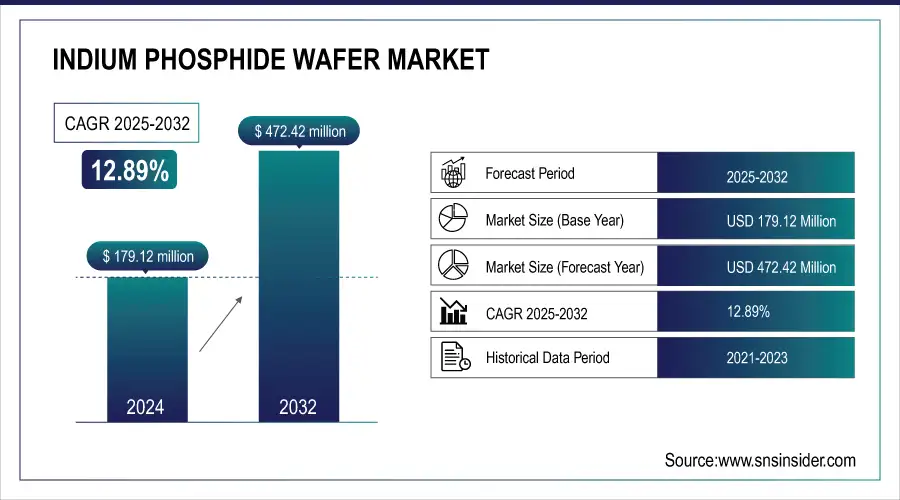
Indium Phosphide Wafer Market Size & Growth:
The Indium Phosphide Wafer Market size was valued at 179.12 Million in 2024 and is projected to reach USD 472.42 Million by 2032, growing at a CAGR of 12.89% from 2025 to 2032.
Indium Phosphide (InP) Wafer Market growth is strongly due to increasing demand for high-speed, low-energy photonic devices in data centers, artificial intelligence (AI), telecommunications and sensing technologies. The high-frequency low-power optoelectronics such as lasers and photodetectors take the advantage of the superior electron mobility and direct bandgap of InP. The ramp-up of 5G and next-gen data transfer is an important driver for InP.
Coherent’s Texas facility represents an important step in domestic semiconductor growth, fueled by a USD 33 million investment from the U.S. government.
To Get more information on Indium Phosphide Wafer Market - Request Free Sample Report
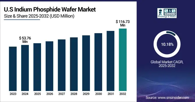
In the United States, the market is also expanding steadily, expected to increase from USD 53.76 Million in 2023 to USD 116.73 million by 2032 at a CAGR of 10.18%. With growing R&D and commercial investments, the global InP wafer market is set for sustained expansion across advanced tech sectors.
In Canada, Université de Sherbrooke developed InP-based solar cells with over 30% efficiency, showcasing national innovation in photonic integration and photovoltaics.
InP Wafer Market Dynamics:
Drivers:
-
Record-Breaking Solar Cell Efficiency Drives Demand for Indium Phosphide Wafers
As the need for high-efficiency solar cells grows, InP’s unique properties make it ideal for use in next-generation photovoltaic technologies. InP's ability to enable high electron mobility and a direct bandgap position it as a critical material for improving the performance of multi junction solar cells.
For example, just recently, researchers from the Fraunhofer ISE and the AMOLF have reached a record efficiency of 36.1% for a multijunction solar cell based on silicon with GaInP and GaAs. The finding highlights how InP can be used in combination to improve the performance of solar cells, particularly in high-efficiency applications.
Restraints:
-
Resistance to Transitioning from Silicon to InP-Based Systems
Numerous industries, including telecommunications and data centers, still depend heavily on silicon-based systems. Making the switch to InP-based technology comes with significant expenses on building new infrastructure and retraining employees. Organizations often resist implementing such changes owing to the required high upfront costs and adjustments to existing workflows. This makes companies consider the immediate challenge of pipelines versus the long-term performance and efficiency benefits of switching to InP. Such resistance can hold back the widespread adoption of InP technology even with its benefits.
Opportunities:
-
Scaling the Future with 6-Inch Indium Phosphide Wafers Unlocking Market Potential
The Indium Phosphide (InP) Wafer Market is entering a transformative phase, with the introduction of the world’s first scalable 6-inch InP wafer manufacturing line by Coherent marking a pivotal shift in production capabilities. As demand surges for AI-driven transceivers, coherent optical communication, and 6G wireless infrastructure, this scale-up in wafer size allows manufacturers to enhance productivity, yield, and performance.
This development increases the number of devices per wafer by a factor of up to four times, resulting in die cost reductions greater than 60%, creating substantial commercial possibilities for next-generation applications including 200G/400G electro absorption modulated lasers (EMLs), high-speed photodetectors and Mach-Zehnder modulators.
Challenges:
-
Extended R&D Cycles Impacting InP Wafer Technology Adoption
The development and testing of Indium Phosphide (InP)-based devices, such as lasers, photodetectors, and transceivers, require extensive research and development (R&D) efforts. These devices must undergo several stages of development, including design, fabrication, and extensive testing for performance, reliability, and compliance with industry standards. Due to the complex nature of InP wafer technologies and the high precision required in their production, the R&D cycles can be lengthy. This prolonged timeline includes multiple iterations of testing and refinement to ensure the devices meet stringent requirements for high-speed data transmission and low-power consumption. As a result, the adoption of InP wafer technologies in industries like telecommunications, Artificial Intelligence, and data centers is slowed down, as businesses are often hesitant to implement new technologies that are still in the lengthy validation phase.
Indium Phosphide (InP) Wafer Market Segment Analysis:
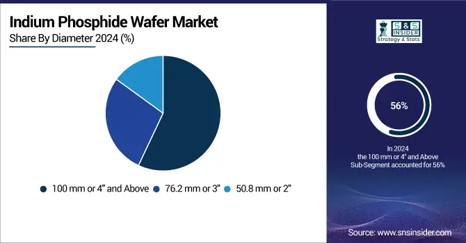
By Diameter
In 2024, the 100 mm (4") segment and higher segment is anticipated to dominate the Indium Phosphide (InP) wafer market, accounting for more than 56% value share of the total industry. The prevalence of High Voltage (HV) and its increased usage for manufacturing high-efficiency optoelectronic devices such as lasers, photodetectors, and transceivers for telecommunication, data centers, and AI infrastructure fueled the largest market size. In addition to accommodating more devices per wafer, larger wafers also increase production efficiency, further driving down per-unit cost and enhancing overall yield.
The 76.2 mm (3") segment of the Indium Phosphide (InP) wafer market is expected to experience the fastest growth from 2025 to 2032. This explosive growth is fueled by demand for small, low-cost wafers that power capabilities across applications we want, such as sensors, high-speed communications, and medical devices. These 3" wafers fill a gap between price and performance in the development of high-end optoelectronic components in support of new technologies such as 5G, automotive connectors, and IoT devices.
By End User
In 2024, the telecommunications segment dominated the Indium Phosphide (InP) wafer market, accounting for approximately 44% of the total revenue. This is driven by the growing need for fast and dependable communication technologies, particularly as 5G networks continue to be rolled out globally and plans for 6G are developed. Indium phosphide (InP) wafers are utilized in the production of optoelectronic elements like lasers, photodetectors, and transceivers that enable sophisticated optical communication systems, which are vital for high-bandwidth data transfer.
The consumer electronics segment is expected to be the fastest-growing sector in the Indium Phosphide (InP) wafer market from 2025 to 2032. The need for low energy consumption, high performance devices is growing with every new mobile devices, electronics and home intelligent systems being introduced into the market, such as smartphones, wearables, smart home products, etc. InP wafers are used to manufacture optoelectronic devices including lasers and photodetectors, which are key technology enablers for advanced sensing, imaging or display technologies in consumer electronics.
Indium Phosphide Wafer Market Regional Overview:
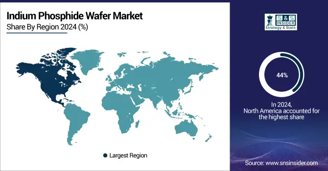
In 2024, North America Region is dominated in the Indium Phosphide (InP) wafer market, accounting for around 44% of global revenue, due to the development of an established semiconductor-manufacturing ecosystem, as well as a broad network of research centers, especially in the US. In North America Region the U.S Country dominated the Indium Phosphide Wafer Market. The U.S. benefits from a strong presence of semiconductor fabrication facilities, fostering innovation in InP-based devices for applications like telecommunications, AI, and photonics. The region's ongoing investments in advanced technologies, such as quantum computing and high-performance computing, continue to drive demand for high-quality InP wafers, ensuring North America's prominent position in the global market.
Get Customized Report as per Your Business Requirement - Enquiry Now
Asia Pacific is projected to be the fastest-growing region in the Indium Phosphide (InP) wafer market during the forecast period with a CAGR 14.66%. The market expansion is due to increasing investments in 5G infrastructure, expansion of the data center network, and growing production house of consumer electronics in China, Vietnam, Japan, South Korea and India. The growing number of telecommunication companies in this region with a well-established supply chain, along with favorable governmental initiatives and the presence of key semiconductor market players adopting Indium Phosphide-based solutions for high-speed data transmission and cutting-edge photonic applications is contributing to the growth of the Indium Phosphide market in this region.
In Asia Pacific Region, the China dominated the Indium Phosphide Wafer Market. The Indium Phosphide (InP) wafer market is dominated by China. China came in first because of its large-scale investments in semiconductors manufacturing, robust government backing with policies such as “Made in China 2025” and fast-growing telecommunications and consumer electronics industries.
Europe maintains a moderate growth position in the Indium Phosphide (InP) Wafer Market, supported by its strong foundation in semiconductor research and advanced technologies. The region shows significant investment in photonics, telecommunications, and data center applications that rely on high-performance InP-based devices. Germany, the UK, and France are leading nations in the development and processing of optoelectronic technologies. With increasing establishment of manufacturing and research facilities, Europe is taking steps to reduce reliance on foreign producers by enhancing its domestic chip-making capabilities. The market is further strengthened by government initiatives aimed at building a resilient and self-sufficient semiconductor ecosystem.
In Latin America and Middle East & Africa Indium Phosphide (InP) wafer market (MEA) is small as compared to the other regions but is likely to experience steady growth, owing to rising investments in telecommunications, data center and emerging technologies. Latin American countries, where demand for InP wafers in optical communications, AI-based applications, is lower than in other regions. The MEA region is also progressively starting to adapt of higher end technologies with nations like UAE and Saudi Arabia aiming for building advanced infrastructure in areas including data center (DC) and optical networks.
Key Players in the Indium Phosphide (InP) Wafer Market are:
Indium Phosphide wafer market Companies include Sumitomo Electric Industries, AXT Inc., IntelliEPI Inc., Wafer Technology Ltd., JX Nippon Mining & Metals Corporation, Ortel, Furuya Metal Co., Ltd., MTI Corporation, PAM-XIAMEN, Beijing JiYa Semiconductor Material Co., Ltd.
Recent Developments:
-
On January 2025, Ortel, a subsidiary of Photonics Foundries, transferred its C-Band indium phosphide (InP) laser diode wafer fabrication from Emcore to the Canadian Photonics Fabrication Centre (CPFC) to enhance capacity and ensure supply continuity.
-
On October 2024, HieFo Corporation announced its participation in the LD Micro Main Event XVII, highlighting its strategic positioning in AI and data center connectivity through high-efficiency indium phosphide (InP) photonic devices. Following its acquisition of EMCORE’s optical core assets, including a world-class North American InP wafer fab, HieFo has solidified its leadership in advanced optoelectronic solutions for next-gen datacom and telecom markets.
| Report Attributes | Details |
|---|---|
| Market Size in 2023 | USD 179.12 Million |
| Market Size by 2032 | USD 472.42 Million |
| CAGR | CAGR of 12.89% From 2024 to 2032 |
| Base Year | 2024 |
| Forecast Period | 2025-2032 |
| Historical Data | 2021-2023 |
| Report Scope & Coverage | Market Size, Segments Analysis, Competitive Landscape, Regional Analysis, DROC & SWOT Analysis, Forecast Outlook |
| Key Segments | • By Diameter (50.8 mm or 2 ", 76.2 mm or 3 ", 100 mm or 4" and Above) • By End User (Consumer Electronics, Telecommunications, Medical, Other End-user Industry Applications) |
| Regional Analysis/Coverage | North America (US, Canada, Mexico), Europe (Eastern Europe [Poland, Romania, Hungary, Turkey, Rest of Eastern Europe] Western Europe] Germany, France, UK, Italy, Spain, Netherlands, Switzerland, Austria, Rest of Western Europe]), Asia-Pacific (China, India, Japan, South Korea, Vietnam, Singapore, Australia,Taiwan, Rest of Asia-Pacific), Middle East & Africa (Middle East [UAE, Egypt, Saudi Arabia, Qatar, Rest of Middle East], Africa [Nigeria, South Africa, Rest of Africa], Latin America (Brazil, Argentina, Colombia, Rest of Latin America) |
| Company Profiles | Key players in the Indium Phosphide wafer market include Sumitomo Electric Industries, AXT Inc., IntelliEPI Inc., Wafer Technology Ltd., JX Nippon Mining & Metals Corporation, Ortel, Furuya Metal Co., Ltd., MTI Corporation, PAM-XIAMEN, Beijing JiYa Semiconductor Material Co., Ltd., and Others |
Get in Touch
