Photomask Repair System Market Report Scope & Overview:
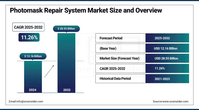
The Photomask Repair System Market size was valued at USD 12.16 billion in 2024 and is expected to reach USD 28.55 billion by 2032, growing at a CAGR of 11.26% over the forecast period of 2025-2032.
Photomask Repair System Market growth is driven by a significant part of the semiconductor manufacturing industry, serving as a major solution that plays a significant role in photomask quality for chip Dense integration. Photomask Repair Equipment is one major piece of photomask repair equipment that offers critical automated defect detection and correction capabilities to maintain high performance within a cost-effective process for photomask fabrication. With more complex semiconductor devices, Semiconductor Photomask Repair Tool drivers are also more complex, and this has triggered innovation in repair techniques.
To Get more information On Photomask Repair System Market - Request Free Sample Report
Of these classifications, the Laser Photomask Repair System Market is particularly popular as it incorporates laser technology, as it allows for a highly precise, efficient, and low-damage repair of photomasks. The growth of the Photomask Repair System Industry is rapid, owing to the rise of the semiconductor industry along with the continuous miniaturization of chips. Recent Photomask Repair System Market Trends Engaging Automation and AI, Diagnostic System of inspection aiding in accurate repair and high throughput. Further, this results in more eco-friendly repair alternatives that reduce waste and enhance sustainability. Hence, the Photomask Repair System Market will maintain the trend and will gain momentum in the future as semiconductor companies seek quality control and yield enhancement by means of advanced photomask repair.
For instance, Bruker continues to lead advancements in photomask repair technology with its FP-III Femto-Pulse Laser System, a third-generation solution designed for high-speed and precision repairs in semiconductor manufacturing.
Photomask Repair System Market Dynamics:
Drivers:
-
EUV Lithography and Smaller Nodes are Fueling Demand for Precise Photomask Repair to Maintain Defect-free Chip Production
Advancements in semiconductor technology, particularly the shift to extreme ultraviolet (EUV) lithography and the development of smaller nodes including 5nm and below, have significantly increased the demand for precise photomask repair systems. Features etched into semiconductors using EUV lithography are finer than what was possible before, but this kind of photomask is also more vulnerable than those of the past to even tiny defects that may lead to a reduced chip. The most recent of such innovations include Intel bringing together the most high-end EUV lithography system in the world. Moreover, at the Paul Scherrer Institute, resolutions below 5nm by EUV lithography have been reported, indicating that extremely high-precision photomask repair technologies are required.
May 2025 – TSMC is still assessing ASML’s High-NA EUV lithography machines, citing high costs and stating its A14 node can progress without them. In contrast, Intel plans to adopt High-NA tools for its future 14A process to gain a competitive edge. ASML has delivered five of these advanced machines so far. High-volume deployment is expected around 2026–2027.
Restraints:
-
High costs and complexity hinder small semiconductor firms from adopting advanced photomask repair, affecting yield.
High capital investment is a significant barrier in the photomask repair system market. Electron-beam and laser systems are among the most advanced repair equipment, and they range in single-unit cost from USD 10 million to USD 35 million, respectively. A complete mask shop for the advanced nodes (45nm or 22nm) will require around USD 60 million up to over USD 100 million. The heavy investments required are hard for small-sized semiconductor manufacturers to obtain, restricting their capital to introduce advanced repair equipment. Furthermore, the operational complexity inherent in operating and maintaining these advanced systems requires expert training, which inevitably raises operational costs. As a result, the smaller players may resort to low-end repair approaches, which may have ripple effects on the performance and wafer yield of semiconductors.
In January 2025, KASFAB Tools inaugurated India’s first semiconductor equipment manufacturing facility in Doddaballapur, Karnataka. The company secured a USD 2.3 million contract and plans to invest USD 30 million over the next 6–12 months to expand operations and set up two more plants. This marks a significant step in boosting India’s semiconductor manufacturing capabilities.
Photomask Repair System Market Segmentation Oulook:
By Type
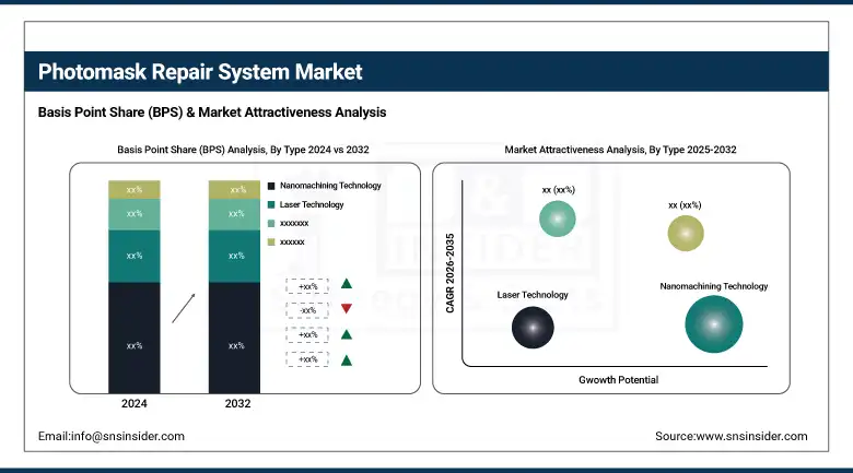
The nanomachining technology segment dominated the market and accounted for 45% of the Photomask Repair System market share in 2024 due to its ability to provide the required extremely fine resolution and accuracy for repairing defects on photomasks used in advanced semiconductor manufacturing. This precision allows the manipulation of nanometric features, which is highly important with so many intricate mask patterns needing to be preserved. Due to its precision, new defects are less likely to be introduced, thus providing high yield and reliability. Due to its efficiency in managing complex repairs, nanomachining has found favor among semiconductor manufacturers targeting the most advanced technology nodes.
Laser technology in photomask repair systems is the fastest-growing segment due to its precision, speed, and non-contact nature. It enable low-touch, high-fidelity repair of mask defects, thereby mitigating the risk of further damage to the surface. It has sufficient capability to aid the move toward smaller feature sizes in the semiconductor manufacturing process due to its ability to manage defects at the nanoscale level. Growing adoption of this technology is fueled by the ability to develop efficient laser sources and control systems for photomask repair, which is critical for advanced node fabrication processes with precision and speed expectations.
By Application
Semiconductor device manufacturers dominate the photomask repair system market, holding 58% of the share in 2024, as they require extremely high-quality photomasks to produce reliable chips. As all masks that are made must be defect-free to maintain high yields and product performance, these manufacturers exercise considerable expense toward repairing systems. With an increase in complexity and miniaturization of semiconductor devices, advanced repair technologies fall under demand. With in-house mask repair, these manufacturers minimize downtime, maintain process control, and speed time-to-market for new semiconductor products.
Mask shops are the fastest-growing application segment in photomask repair systems, driven by the outsourcing trend in semiconductor manufacturing. These providers, which service photomasks for different semiconductor manufacturers, provide a cost-efficient and more effective way to get photomasks repaired and maintained. As photomasks become more intricate, mask shops spending on the advanced repair technologies they need to meet demand, thus driving fast growth. This level of specialization and expertise has led to the prominence of mask shops that provide repair services as semiconductor companies streamline and focus their efforts on core manufacturing, fueling demand for advanced repair systems within this space.
Photomask Repair System Market Regional Analysis:
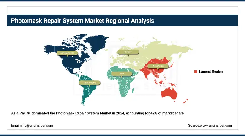
Asia-Pacific holds the largest share of the photomask repair system market, accounting for 42% of the global market. Such dominance is supported by key semiconductor fabrication centers in the nations of China, South Korea, Japan, and Taiwan. The high investments in the advanced photolithography and the semiconductor fabrication technologies by these countries are expected to create opportunities for photomask repair systems. Moreover, a rapidly growing market for new mass production electronic designs due to strong government support and well-established large-scale foundries, and China's steadily growing electronics sector, drives the region's market growth. The strong cost advantage in production capabilities and the increasing domestic demand for consumer electronics in the region further solidify its position as a global leader.
Get Customized Report as per Your Business Requirement - Enquiry Now
India is the fastest-growing country in the Asia-Pacific photomask repair system market, driven by strong government support through initiatives including the PLI scheme. Increasing demand for photomask repair technologies due to the growth of the electronics and semiconductor sectors in the country. This is launching innovation with a bigger talent pool of engineers with a lot of experience and new R&D partnerships. All these factors are keeping India an upcoming semiconductor manufacturing hub.
Europe is the fastest-growing region in the photomask repair system market, driven by expanding semiconductor fabrication facilities and growing investments in microelectronics. In line with the EU strategy for semiconductor independence, Germany, France, and the Netherlands are improving their chip production capabilities. Rapid growth is driven by the expanding role of global equipment manufacturers and the rising need for photomask repair in photolithography processes. Europe is expected to be the next growth engine in the upcoming period, with green technologies and smart electronics dominating its focus, thus boosting demand in the market.
North America holds a significant share in the photomask repair system market owing to the well-established semiconductor manufacturing base, advanced R&D infrastructure, and the presence of major technology companies. The U.S. and Canada are early adopters of emerging lithography, photomask repair technologies with an initial focus on integrated circuit manufacture. Moreover, positive, support-driven, and capital-invested activities in semiconductor production by local governments strengthen the demand in the region. North America is not the largest market, but its mature ecosystem and technological position will keep it competitive and relevant in the global photomask market.
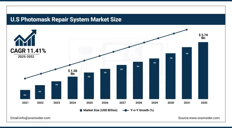
The U.S. Photomask Repair System market is projected to grow from USD 1.58 billion in 2024 to USD 3.74 billion by 2032, registering a CAGR of 11.41%. Due to a strong semiconductor manufacturing base in the country, and increasing demand for advanced photolithography solutions, Ongoing innovation within chip design and favorable government policies, especially the CHIPS and Science Act, are also driving growth in the market by providing support to different sectors.
Photomask Repair System Companies are:
Ingersoll Rand, SPX Flow, Alfa Laval, Grundfos, IDEX Corporation, Schlumberger Limited, Weir Group PLC, KSB Group, Sulzer Ltd., and Flowserve Corporation.
Recent Development:
In October 2024: Carl Zeiss SMT GmbH unveiled the MeRiT MG neo, an advanced photomask repair system tailored for mature technology nodes as small as 45 nm. Engineered with a modular and space-saving architecture, the system delivers high throughput and enhanced serviceability. It addresses the growing need for economical repair solutions, particularly in the IoT and automotive sectors, where maintaining cost-efficiency is critical.
In February 2024: HTL Co. Japan Ltd. secured a major order for its Pictor2323 photomask repair system from a leading semiconductor manufacturer in Asia. The latest iteration features a reengineered mechanical design that minimizes installation space and boosts operational performance. This advancement significantly enhances both efficiency and cost-effectiveness, aligning with the evolving demands of high-volume chip production.
In March 2024: Hitachi High-Tech Corporation launched a next-generation photomask inspection platform, integrating dark-field laser scattering and Differential Interference Contrast (DIC) technologies. This innovative system improves defect detection accuracy on both mask surfaces, contributing to higher yields and greater precision in semiconductor fabrication processes.
| Report Attributes | Details |
|---|---|
| Market Size in 2024 | USD 12.16 Billion |
| Market Size by 2032 | USD 28.55 Billion |
| CAGR | CAGR of 11.26% From 2025 to 2032 |
| Base Year | 2024 |
| Forecast Period | 2025-2032 |
| Historical Data | 2021-2023 |
| Report Scope & Coverage | Market Size, Segments Analysis, Competitive Landscape, Regional Analysis, DROC & SWOT Analysis, Forecast Outlook |
| Key Segments | • By Type (Laser Technology, Focused Ion Beam (FIB) Technology, Nanomachining Technology) • By Application (Semiconductor Device Manufacturers, Mask Shops) |
| Regional Analysis/Coverage | North America (US, Canada, Mexico), Europe (Germany, France, UK, Italy, Spain, Poland, Turkey, Rest of Europe), Asia Pacific (China, India, Japan, South Korea, Singapore, Australia, Rest of Asia Pacific), Middle East & Africa (UAE, Saudi Arabia, Qatar, South Africa, Rest of Middle East & Africa), Latin America (Brazil, Argentina, Rest of Latin America) |
| Company Profiles | Ingersoll Rand, SPX Flow, Alfa Laval, Grundfos, IDEX Corporation, Schlumberger Limited, Weir Group PLC, KSB Group, Sulzer Ltd.,Flowserve Corporation. |
Frequently Asked Questions
The Asia-Pacific region dominated the Photomask Repair System market in 2024.
The “Nanomachining Technology” segment dominated the Photomask Repair System market.
EUV lithography and smaller nodes are fueling demand for precise photomask repair to maintain defect-free chip production.
The Photomask Repair System market was USD 12.16 billion in 2024 and is expected to reach USD 28.55 billion by 2032.
The Photomask Repair System market is expected to grow at a CAGR of 11.26% from 2025-2032.
Get in Touch
