Extreme Ultraviolet (EUV) Lithography Market Report Scope & Overview:
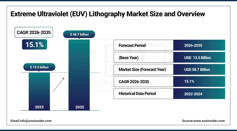
The Extreme Ultraviolet (EUV) Lithography Market was valued at USD 13.5 billion in 2025 and is expected to reach USD 58.7 billion by 2035, growing at a CAGR of 15.1% from 2026-2035.
The Extreme Ultraviolet (EUV) Lithography Market represents one of the most technologically advanced and strategically important segments of the global semiconductor manufacturing industry. EUV lithography utilizes light with a wavelength of 13.5 nanometres to pattern ultra-fine semiconductor features, enabling the production of cutting-edge chips at process nodes of 3nm, 2nm, and beyond. As transistor dimensions continue to shrink, EUV technology has become indispensable for manufacturing high-performance processors, AI accelerators, advanced memory devices, and next-generation mobile chipsets. Despite the substantial capital investment required for EUV systems, which are among the most complex and expensive industrial machines ever developed, semiconductor manufacturers continue to expand deployment due to the growing demand for advanced silicon.
ASML's 2024 annual report documents total EUV system revenue exceeding EUR 10 billion, with an order backlog representing over 12 months of production capacity. The Semiconductor Industry Association projects that global semiconductor capital equipment spending will reach USD 100 billion by 2026, with EUV lithography representing the highest-value single equipment category in advanced node fab construction.
EUV Lithography Market Size and Forecast
-
Market Size in 2025: USD 13.5 Billion
-
Market Size by 2035: USD 58.7 Billion
-
CAGR: 15.1% from 2026 to 2035
-
Base Year: 2025
-
Forecast Period: 2026-2035
-
Historical Data: 2022-2024
To Get more information on Extreme Ultraviolet (EUV) Lithography Market - Request Free Sample Report
EUV Lithography Market Trends
-
High-NA EUV ASML's next-generation system with 0.55 numerical aperture versus the current 0.33 NA is beginning commercial deployment, enabling patterning of sub-2nm features that conventional EUV cannot resolve.
-
Multi-patterning EUV techniques are extending current EUV systems' useful life at advanced nodes by applying EUV exposure multiple times to achieve feature pitches below single-exposure limits.
-
EUV pellicle development thin membranes protecting photomasks from particle contamination has reached transmission efficiencies above 90%, removing a major barrier to production adoption of pellicle-protected EUV masks.
-
Stochastic defects random pattern failures caused by EUV photon shot noise at extremely low doses remain the leading technical challenge for EUV yield at the most advanced nodes, driving research investment in resist materials and exposure optimization.
-
AI-optimized chip layouts are being adopted by leading foundries to reduce the number of EUV exposure passes required per chip layer, improving wafer throughput and reducing per-chip EUV fabrication cost.
-
EUV photomask inspection technology requiring actinic EUV inspection at 13.5nm wavelength rather than visible light is developing as a critical quality control bottleneck whose resolution will improve production yields at sub-3nm nodes.
-
Government semiconductor sovereignty programs in the U.S., EU, Japan, South Korea, and India are funding advanced fab construction that includes EUV lithography equipment procurement.
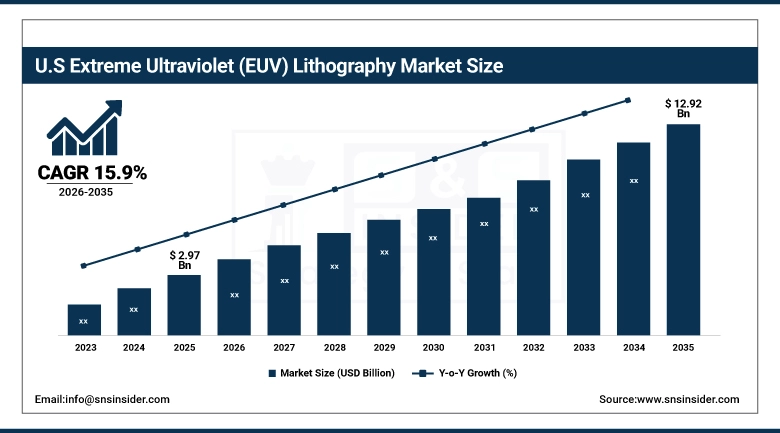
U.S. EUV Lithography Market was valued at USD 2.97 billion in 2025 and is expected to reach USD 12.92 billion by 2035, growing at a CAGR of 15.9% from 2026-2035.
North America is positioned as the fastest-growing EUV Lithography Market region, with the United States driving this trajectory through the CHIPS and Science Act's USD 52 billion investment commitment that is reshaping domestic advanced semiconductor manufacturing capacity at a pace not seen since the 1990s. Intel's Ohio fab complex which will ultimately house two EUV-equipped fabrication facilities TSMC's Arizona fabs running N3 and N2 processes, Samsung's Texas fab, and Micron's Idaho memory expansion each represent substantial EUV equipment procurement that was not present in the U.S. market two years prior. The U.S. government's recognition that advanced semiconductor manufacturing is a national security imperative has converted what was previously a 100% Asia-Pacific-concentrated EUV capability into a genuinely global equipment deployment picture and the capital committed to domestic EUV capability in the U.S. will sustain the fastest regional CAGR through the forecast period.
The U.S. Department of Commerce's CHIPS Act office has disbursed over USD 28 billion in preliminary agreements to Intel, TSMC, Samsung, Micron, and GlobalFoundries for domestic fab construction, with EUV-capable advanced node facilities representing the majority of the committed investment. Intel's 18A process node using High-NA EUV and novel backside power delivery represents the U.S.-designed technology that could restore American leadership in advanced semiconductor manufacturing.
EUV Lithography Market Segment Analysis
-
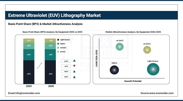
By Equipment, Light Source dominated with ~39% share in 2025; Mask segment expected to grow at the fastest CAGR of ~16.4%.
-
By End-User, Integrated Device Manufacturers (IDMs) dominated with ~63% share in 2025; Foundries fastest growing at ~16.06% CAGR.
By Equipment: Light Source dominates, Mask growing fastest at 16.4% CAGR
The Light Source segment held approximately 39% of the EUV Lithography Market in 2025, reflecting the centrality and commercial scale of the laser-produced plasma (LPP) light source technology that powers ASML's EUV systems. The EUV light source where high-power CO2 lasers irradiate molten tin droplets to create plasma that emits 13.5nm wavelength radiation is both the enabling technology and the primary cost driver of EUV lithography systems. Companies including Ushio Inc. and Gigaphoton Inc. supply the laser components and driver technologies that power ASML's light source modules. The source's power output directly determines wafer throughput per tool, making source power improvement one of the most commercially valuable technical advances in the EUV industry. ASML's current production EUV tools generate 250 watts of EUV power; High-NA EUV tools are targeting 600 watts for equivalent throughput at the new tool's resolution capability. Each incremental source power improvement translates directly into wafer output per machine-hour, the fundamental unit of EUV's commercial value.
The Optics segment encompassing the collector mirrors, illuminator mirrors, and projection optics that direct, shape, and focus EUV radiation onto the wafer surface is a critical enabler of EUV system performance whose development is dominated by ZEISS Group's semiconductor technology division. EUV optical components require aspherical mirror surfaces accurate to better than 0.1nm roughness a polishing precision that puts them among the most accurately manufactured objects on Earth. ZEISS and ASML have developed an exclusive supply relationship for EUV optics that represents a strategic dependency for global semiconductor equipment manufacturing that both companies have invested substantially to sustain.
The Mask segment is projected to grow at the highest CAGR of approximately 16.4% during the forecast period, driven by EUV photomask's technical evolution alongside the process nodes it enables. As chip layouts advance to 2nm and below, the EUV photomask must pattern features with absolute dimensional accuracy measured in fractions of a nanometer a specification that drives continuous investment in mask blank substrate quality, reflective multilayer coating uniformity, absorber material optimization, and defect inspection capability. Major photomask suppliers including Toppan Photomasks, Dai Nippon Printing, and Photronics are each investing substantially in EUV mask production capability. ZEISS's collaboration with ASML on EUV pellicle technology protecting masks from particle contamination during exposure is enabling longer mask lifetimes and improved production yield in high-volume EUV fab environments.
ASML's 2024 Technology Roadmap presentation documents that High-NA EUV systems ordered by Intel, TSMC, and Samsung are the highest-value capital equipment orders in semiconductor manufacturing history, with each system priced above USD 300 million. The EUV photomask market is projected by SEMI to grow at above-market rates through 2027 as leading foundries qualify new mask sets for each successive advanced process node.
By End-User: IDMs dominate, Foundries growing fastest at 16.06% CAGR
Integrated Device Manufacturers held approximately 63% of the EUV Lithography Market in 2025, reflecting the dominant EUV procurement of Samsung and Intel both IDMs that design and manufacture their own chips alongside Micron and SK Hynix in memory applications. Samsung's EUV adoption across its foundry and memory operations simultaneously makes it both the world's second-largest EUV tool user and a significant EUV-based competitor to TSMC in the foundry market. Intel's extraordinary EUV investment pursuing the Intel Foundry Services strategy that requires competitive process technology at 18A and beyond represents a major IDM commitment to EUV that will sustain this segment's scale through the forecast period. Memory manufacturers' adoption of EUV for DRAM patterning specifically for the most critical layers in each DRAM generation adds a high-volume consumption category that foundry EUV fabs do not serve.
The Foundries segment is projected to grow at the fastest CAGR of approximately 16.06% throughout the forecast period, driven by the structural shift of the global semiconductor industry from IDM-dominated to fabless-foundry model that has been compounding for two decades. As more chip design companies adopt fabless models outsourcing manufacturing to specialized foundries rather than building and operating their own fabs foundry demand for EUV capacity scales with the aggregate design output of thousands of fabless companies rather than the internal product roadmaps of a handful of IDMs. TSMC which controls approximately 55% of the global foundry market and serves essentially every leading-edge fabless chip designer is the dominant EUV foundry customer, but Samsung Foundry, Intel Foundry Services, and GlobalFoundries are each building EUV-capable capacity that will collectively expand foundry EUV consumption as a share of total market.
EUV Lithography Market Regional Analysis
|
Region |
Major Country |
Share within Region (%) |
|---|---|---|
|
Asia Pacific |
Taiwan |
42% |
|
North America |
United States |
92% |
|
Europe |
Netherlands |
55% |
|
Middle East & Africa |
Israel |
45% |
|
Latin America |
Brazil |
50% |
Asia Pacific EUV Lithography Market Insights
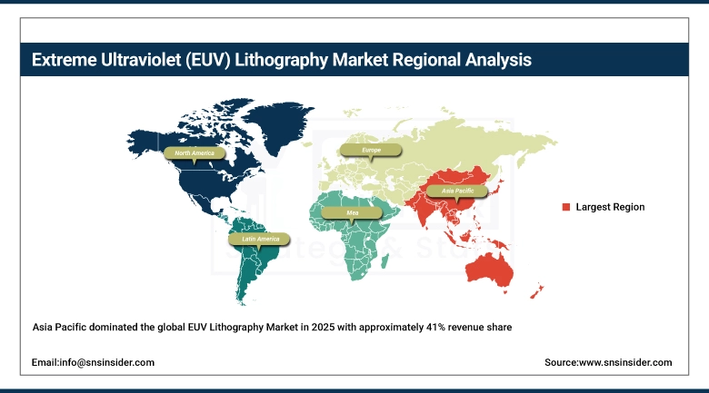
Asia Pacific dominated the global EUV Lithography Market in 2025 with approximately 41% revenue share, anchored by Taiwan's extraordinary fab density TSMC's Hsinchu and Tainan fab complexes house the world's most advanced EUV production capacity alongside South Korea's Samsung and SK Hynix EUV operations and Japan's growing government-supported advanced semiconductor program. Taiwan is arguably the single most strategically important location in global semiconductor manufacturing: TSMC's fabs produce the vast majority of the world's most advanced chips, and their EUV tool population represents the world's highest-value concentration of lithography equipment. South Korea's two EUV-intensive companies Samsung with both foundry and memory EUV fabs and SK Hynix with memory EUV operations create a dual-company regional demand that sustains Korea's position as the world's second-largest EUV market by tool count.
TSMC reported in its 2024 annual report that it had deployed over 100 EUV tools across its production facilities, with additional tools on order for its expanding 2nm and N2P capacity at Kaohsiung Science Park. Japan's Rapidus a government-supported consortium targeting 2nm chip manufacturing by 2027 has signed a collaboration agreement with IBM and IMEC for EUV process development, with ASML EUV tool procurement already underway.
Get Customized Report as per Your Business Requirement - Enquiry Now
North America EUV Lithography Market Insights
North America is the fastest-growing regional EUV Lithography Market with an estimated CAGR of approximately 16.3% the highest of any region driven by the CHIPS Act-funded fab construction wave that is establishing EUV-capable advanced manufacturing in the U.S. for the first time at commercial scale. Intel's Ohio fab complex described as the largest semiconductor manufacturing campus in U.S. history will house EUV tools for its 18A and beyond process nodes that Intel is developing to re-establish global process leadership. TSMC Arizona's Phase 1 (N4 process) is ramping with immersion lithography, while Phase 2 (N3) will incorporate EUV, and Phase 3 (N2) will be EUV-intensive creating a multi-year EUV equipment procurement profile in Arizona alone. Samsung Austin's advanced node expansion similarly represents EUV tool installations in the U.S. market.
The U.S. CHIPS Act's Creating Helpful Incentives to Produce Semiconductors program has awarded USD 8.5 billion to Intel, USD 6.6 billion to TSMC, and USD 6.4 billion to Samsung investments that directly fund EUV-capable fab construction and equipment procurement in the U.S. market.
Europe EUV Lithography Market Insights
Europe's position in the EUV Lithography Market is unique: while its fab capacity is modest compared to Asia Pacific and North America, it hosts ASML the market's sole equipment supplier in the Netherlands, alongside ZEISS (optics) in Germany, making Europe the center of EUV technology development even as most production capacity is elsewhere. The European Chips Act's EUR 43 billion investment commitment aims to double Europe's global semiconductor market share to 20% by 2030, with Intel's planned Magdeburg fab as the most ambitious European advanced semiconductor investment. Germany's Saxony region home to Intel's planned 10nm-class fab and Bosch's 12-inch power chip facility represents the leading edge of European semiconductor manufacturing ambition. The EU's recognition that extreme dependence on Asian and American chip supply creates strategic vulnerability is driving investment in European advanced semiconductor capabilities that will include EUV tool deployment.
ASML's corporate headquarters in Veldhoven, Netherlands employs over 40,000 people globally and represents Europe's most commercially and strategically significant technology company. The Dutch government's export control coordination with the U.S. that restricts ASML EUV sales to China has reshaped global EUV equipment trade flows in ways that directly affect where EUV capacity is being built.
Middle East & Africa and Latin America EUV Lithography Market Insights
Neither Middle East & Africa nor Latin America currently host significant EUV lithography deployments, as the capital intensity and supply chain complexity of EUV fabs require the semiconductor industry ecosystems component suppliers, materials specialists, equipment service networks, and trained engineering talent that have concentrated in East Asia, the U.S., and Europe over decades of industry development. However, Israel's Tower Semiconductor a significant specialty foundry serving automotive, industrial, and photonic chip markets represents the MEA region's most sophisticated semiconductor manufacturing presence. Saudi Arabia's Vision 2030 technology diversification includes exploratory semiconductor ecosystem development that could eventually create EUV-relevant investment, though timelines remain distant from commercial EUV deployment. Latin America has no current EUV market presence.
EUV Lithography Market Growth Drivers:
AI chip demand and advanced node scaling requirements driving extraordinary EUV lithography market growth globally
The EUV lithography market's 15.1% CAGR is fundamentally driven by the AI revolution's semiconductor demand implications. Training a frontier large language model requires clusters of tens of thousands of advanced AI accelerators GPUs and custom AI chips like Google's TPUs and Amazon's Trainium each of which is fabricated on advanced process nodes where EUV lithography is the enabling patterning technology. As AI model scale doubles roughly annually following current capability development trajectories, the aggregate advanced chip demand grows proportionally, creating growing EUV equipment demand. The smartphone market's continued advancement to 3nm and 2nm mobile processors, the data center buildout that cloud computing and AI inference require, and the automotive industry's growing content of advanced driver assistance chips each add independent demand vectors to the EUV market's growth foundation.
NVIDIA's H100 GPU the dominant AI training accelerator is manufactured on TSMC's 4nm N4 process that uses EUV lithography for critical layers. NVIDIA's projected GPU revenue exceeding USD 100 billion annually sustains fab utilization at TSMC that directly translates to EUV tool utilization. The Semiconductor Industry Association projects that AI chip demand alone could consume 30% of global advanced node wafer capacity by 2027.
EUV Lithography Market Restraints:
ASML supply monopoly and China export restrictions creating EUV lithography market access and geopolitical challenges
The EUV lithography market operates under a supply structure with no parallel in high-technology manufacturing: a single company in a single country produces every EUV tool in existence, and the supply of that tool is subject to export controls coordinated between the Dutch and U.S. governments. ASML's production capacity constrained by the complexity of integrating thousands of precision components including ZEISS optics, laser systems, and semiconductor wafer handling mechanisms limits annual tool output to approximately 50-60 EUV systems per year, creating allocation constraints that lead chipmakers to queue years in advance for tool delivery. The Dutch government's export control compliance means that China which has the capital and ambition to be a major EUV customer cannot import EUV tools, creating geopolitical tensions that affect global semiconductor supply chain strategy.
EUV Lithography Market Opportunities:
High-NA EUV commercialization and government fab investment programs creating transformative EUV lithography growth opportunities
High-NA EUV ASML’s 0.55 numerical aperture NXE:5000 system represents the most significant EUV technology advancement since EUV's original commercialization. By increasing the numerical aperture from 0.33 to 0.55, High-NA EUV nearly doubles the resolution capability, enabling single-exposure patterning of sub-2nm features that current EUV achieves only through complex multi-patterning techniques. Intel has committed to be the first commercial High-NA EUV adopter for its 18A process, with the first production tool installed at Intel's Hillsboro, Oregon development facility. As High-NA systems reach production volumes through, each tool displacing current-generation EUV systems at leading-edge fabs will generate incremental market revenue at per-tool prices exceeding USD 300 million significantly higher than current EUV system pricing.
Recent Developments:
-
2026: ASML shipped its 50th High-NA EUV (NXE:5000) system to Intel Foundry Services' Ohio fab campus, marking the first High-NA EUV installation in a high-volume manufacturing environment outside ASML's customer demonstration facilities, with Intel reporting successful patterning of 12nm metal pitch features in early production qualification wafer lots.
-
2025: TSMC began risk production on its N2 (2nm) process at the Baoshan fab in Hsinchu, Taiwan, marking the first commercial production of 2nm chips a milestone requiring 20+ EUV exposure passes per chip in the most critical patterning layers with Apple confirmed as the first production customer for N2 process wafers.
-
2025: Intel and ZEISS announced a co-investment program to accelerate EUV pellicle technology deployment across Intel's 18A production line, with pellicle adoption expected to extend EUV mask lifetimes by 3x and reduce mask replacement costs by USD 150,000 per mask set per 1,000 wafer runs in high-volume manufacturing environments.
EUV Lithography Market Key Players
Some of the Extreme Ultraviolet (EUV) Lithography Market Companies
-
ASML Holding NV
-
Taiwan Semiconductor Manufacturing Company (TSMC)
-
Samsung Electronics Co., Ltd.
-
Intel Corporation
-
SK Hynix Inc.
-
Micron Technology Inc.
-
ZEISS Group (Carl Zeiss AG)
-
Toppan Photomasks Inc.
-
Dai Nippon Printing Co., Ltd. (DNP)
-
Photronics Inc.
-
AGC Inc.
-
Ushio Inc.
-
Gigaphoton Inc.
-
Synopsys Inc.
-
Cadence Design Systems Inc.
-
Applied Materials Inc.
-
Tokyo Electron Ltd.
-
KLA Corporation
-
Lam Research Corporation
-
Entegris Inc.
Extreme Ultraviolet (EUV) Lithography Market Report Scope:
| Report Attributes | Details |
|---|---|
| Market Size in 2025 | USD 13.5 Billion |
| Market Size by 2035 | USD 58.7 Billion |
| CAGR | CAGR of 15.1% From 2026 to 2035 |
| Base Year | 2025 |
| Forecast Period | 2026-2035 |
| Historical Data | 2022-2024 |
| Report Scope & Coverage | Market Size, Segments Analysis, Competitive Landscape, Regional Analysis, DROC & SWOT Analysis, Forecast Outlook |
| Key Segments | • By Equipment (Light Source, Optics, Mask, Others) • By End Use (Integrated Device Manufacturer (IDM), Foundries) |
| Regional Analysis/Coverage | North America (US, Canada), Europe (Germany, UK, France, Italy, Spain, Russia, Poland, Rest of Europe), Asia Pacific (China, India, Japan, South Korea, Australia, ASEAN Countries, Rest of Asia Pacific), Middle East & Africa (UAE, Saudi Arabia, Qatar, South Africa, Rest of Middle East & Africa), Latin America (Brazil, Argentina, Mexico, Colombia, Rest of Latin America). |
| Company Profiles | ASML Holding NV, Taiwan Semiconductor Manufacturing Company (TSMC), Samsung Electronics Co., Ltd., Intel Corporation, SK Hynix Inc., Micron Technology Inc., ZEISS Group (Carl Zeiss AG), Toppan Photomasks Inc., Dai Nippon Printing Co., Ltd. (DNP), Photronics Inc., AGC Inc., Ushio Inc., Gigaphoton Inc., Synopsys Inc., Cadence Design Systems Inc., Applied Materials Inc., Tokyo Electron Ltd., KLA Corporation, Lam Research Corporation, Entegris Inc. |
Frequently Asked Questions
Asia Pacific dominated; North America is the fastest growing at approximately 16.3% CAGR.
IDMs dominated with approximately 63% share; Foundries are the fastest growing at ~16.06% CAGR.
The Light Source segment dominated with approximately 39% share; Mask is the fastest growing at ~16.4% CAGR.
The EUV Lithography Market was valued at USD 13.5 billion in 2025.
The EUV Lithography Market is expected to grow at a CAGR of 15.1% from 2026 to 2035.
Get in Touch
