Semiconductor Dielectric Etching Equipment Market Size Analysis:
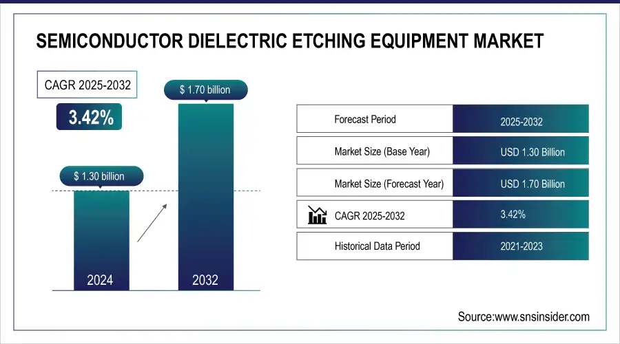
The Semiconductor Dielectric Etching Equipment Market Size was valued at USD 1.30 billion in 2024 and is expected to reach USD 1.70 billion by 2032 and grow at a CAGR of 3.42% over the forecast period 2025-2032.
To Get more information On Semiconductor Dielectric Etching Equipment Market - Request Free Sample Report
The worldwide Semiconductor Dielectric Etching Equipment market is experiencing stable growth based on enhanced demand for advanced semiconductor nodes, chip complexity growth, and continued foundry and IDM investments. The migration towards smaller geometries and 3D architecture necessitates the demand for accurate dielectric etching processes, and hence this segment is pivotal in realizing high-performance, high-density semiconductor devices in a range of end-use applications.
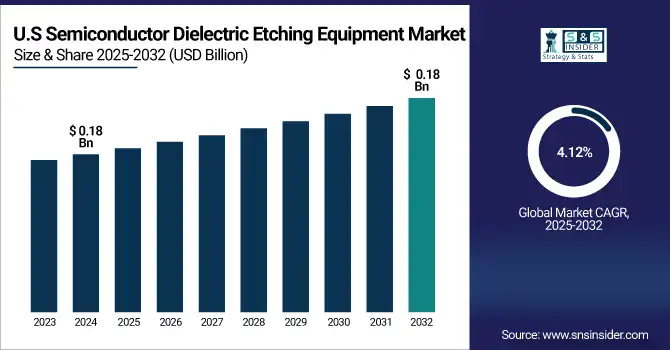
The U.S. Semiconductor Dielectric Etching Equipment Market size was USD 0.18 billion in 2024 and is expected to reach USD 0.25 billion by 2032, growing at a CAGR of 4.12% over the forecast period of 2025–2032.
The U.S. Semiconductor Dielectric Etching Equipment market is witnessing steady growth, aided by renewed domestic chip production and augmented federal investment in semiconductor facilities. Advances in technology and the momentum behind next-generation nodes are propelling demand for high-precision etching solutions, especially among advanced foundries and integrated device manufacturers in the country's growing semiconductor ecosystem.
TSMC's N2 node is expected to provide a 30% improvement in power efficiency over its 3nm predecessor, continuing the company's legacy of delivering power-efficient chips.
Semiconductor Dielectric Etching Equipment Market Dynamics
Key Drivers:
-
Increasing Demand for Advanced Semiconductor Nodes and High-Density Chips Accelerates Growth in the Market.
The demand for high-performance computing, AI, 5G and edge devices is leading to the need for smaller, more complex semiconductor nodes. With chipmakers moving to sub-7nm and 3nm nodes, dielectric etching has risen to be of paramount importance for the formation of the complex multi-layer structures with superior precision and selectivity. Advanced dielectric etch tools are required to maintain etch accuracy without damage to the underlying layers. This development is forcing both foundries and IDMs to purchase advanced & state of art etch systems with ability to support the next generation of architectures. The development of 3D stack and FinFETs has further elevated the importance of dielectric etch tools in advanced semiconductor fabrication.
Samsung has begun mass production of chips using its optimized 3nm process technology, featuring Gate-All-Around (GAA) architecture. This process achieves 45% reduced power usage, 23% improved performance, and a 16% smaller surface area compared to the previous 5nm process.
Restrain:
-
Supply Chain Disruptions and Semiconductor Material Shortages Hinder the Availability of Dielectric Etching Equipment.
Critical material such as specialty gases, wafers and components for etch system fabrication are in short supply and are delaying manufacturing and installation of equipment. Compounding these delays are global logistics issues, which reduce the amount of new etching tools in the market. This leads to longer lead times for semiconductor fabs seeking to add or enhance their capacity, and thus to slower expansion of the dielectric etching equipment market and typically higher costs of operation for companies that use the etchers.
Opportunities:
-
Growing Government Investments in Domestic Semiconductor Fabs Create New Growth Opportunities for Dielectric Etching Equipment Providers.
Initiatives such as the U.S. CHIPS Act and the EU Chips Act offer incentives and subsidies for constructing and enhancing high-end fabs, which demands more advanced etch equipment.Such government-sponsored programs tend to favor technology independence and favor high-end node manufacturing, which depends significantly on accurate dielectric etching. Semiconductor dielectric etching equipment market trends provides a perfect setting for equipment vendors to extend their market footprint, establish strategic alliances with new fabs, and promote innovation in etching processes designed for advanced semiconductor applications.
Challenges:
-
Technological Complexity and Yield Sensitivity Pose Major Challenges to the Growth.
Dielectric etching is more and more demanding as the device dimensions are reduced and the material stacks are more complex. At the advanced nodes, it becomes more and more difficult to control the etching uniformly across the wafer surfaces, while simultaneously maintaining selectivity between various layers, and not causing plasma damage. These technical requirements exacerbate process variation and defect risk, which affect chip yield and fab profitability. Moreover, etch recipes need to be tailored for each new node and for each device architecture, thus ongoing R&D and process development is needed. This increasing complexity curtails equipment suppliers’ ability to provide the proven, scalable solutions needed for advanced semiconductor manufacturing.
Semiconductor Dielectric Etching Equipment Market Segment Analysis:
By Type
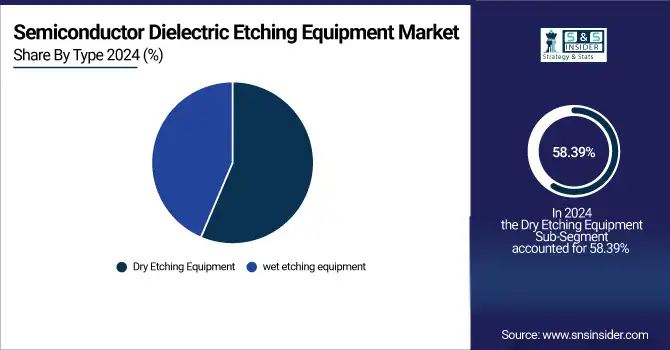
Dry Etching Equipment segment dominated the semiconductor dielectric etching market, with a revenue share of 58.39% in 2024, due to its accuracy, scalability, and compatibility with advanced nodes below 7nm. Lam Research and Tokyo Electron have introduced state-of-the-art plasma etchers that can support 3D NAND and FinFET architectures. In 2023, Lam Research introduced its "Versys Metal Etch" system specific to high aspect-ratio applications, further solidifying its position within dry etch. The relentless march toward miniaturized and multi-layered ICs renders dry etching critical, as it follows a trend of worldwide developments in AI, HPC, and 5G semiconductor fabrication requiring highly selective and anisotropic etch processes.
The wet etching equipment market is anticipated to expand at the fastest CAGR of 4.40% during 2025-2032, driven by its benefits in isotropic etching, cost competitiveness, and use in legacy and specialty semiconductor manufacturing. New developments, including SCREEN Semiconductor Solutions' introduction of cutting-edge wet cleaning and etch tools in 2023, highlight innovation within this arena. Wet etching continues to be essential in compound semiconductors and MEMS devices, which are increasingly being adopted in automotive and IoT applications. Its expansion supplements the dielectric etching equipment market by providing etch solutions where dry etching is financially prohibitive or technically constrained, particularly in mature node manufacturing.
By Application
Foundries dominated the semiconductor dielectric etching equipment market share of 54.09% in 2024 due to strong demand for advanced chips by fabless firms and hyperscale customers. Large foundries such as TSMC and GlobalFoundries are increasing capacity with massive investment in sub-5nm process nodes. TSMC, for instance, partnered with Applied Materials to incorporate next-generation dielectric etching systems into its 3nm and 2nm fabs. The growing intricacy of multi-patterning and 3D device architectures necessitates exacting etching techniques, where sophisticated etch equipment becomes crucial for foundries. This enhances the dominance of the segment in the entire market, particularly in the context of the global expansion of the semiconductor supply chain.
The Integrated Device Manufacturers (IDMs) segment will grow at the fastest CAGR of 4.51% during 2025–2032, led by vertical integration strategies and increased investments in localized manufacturing. Top IDMs such as Intel and Samsung have increased capital spending to increase domestic fabrication capacity. Intel's investment in Lam Research's newest dielectric etch tools in its Ohio fabs highlights the drive toward internal control of process technologies. As IDMs focus more on advanced node capabilities and specialized chip architectures, the demand for high-precision dielectric etching equipment increases. This makes IDMs a major semiconductor dielectric etching equipment market growth.
Semiconductor Dielectric Etching Equipment Market Regional Overview:
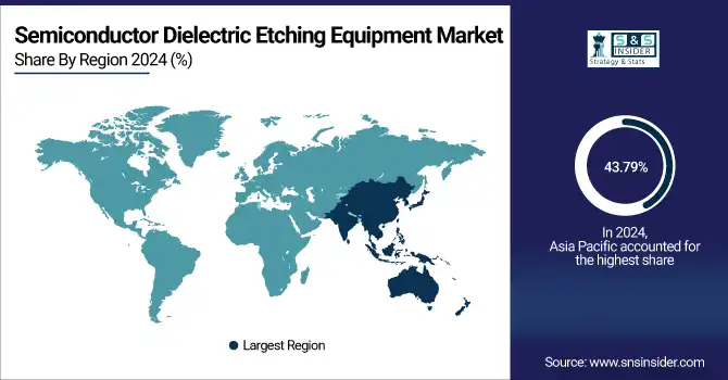
Asia Pacific dominated the semiconductor dielectric etching equipment industry with 43.79% market share in 2024, spearheaded by the dominance of semiconductor production clusters such as Taiwan, South Korea, and China. Heavy industry giants such as Tokyo Electron and Hitachi High-Tech continue to roll out sophisticated dielectric etch systems for sub-5nm production. TSMC and Samsung's continuous fab expansions further support regional demand. The concentration of IDMs and foundries in the region, as well as government-supported semiconductor initiatives, makes Asia Pacific the primary market for dielectric etch equipment that corresponds to advanced node transitions and high-volume chip production.
Get Customized Report as per Your Business Requirement - Enquiry Now
China dominated the Asia Pacific semiconductor dielectric etching equipment market on account of its large-scale semiconductor manufacturing expansion, robust government initiatives, and growing investments in indigenous foundries such as SMIC. This fueling demand for sophisticated etching tools to complement domestic chip making.
North America is expected to expand at the fastest CAGR of 4.82% between 2025 and 2032, driven by robust investments in local semiconductor fabrication and R&D. Lam Research and Applied Materials are among the companies that continue to release future-generation dielectric etching platforms that enable U.S.-based fabs. Intel's expansion plans and the U.S. CHIPS Act are driving local demand for state-of-the-art etch solutions. This expansion is further augmented by strategic supply chain changes and technological leadership in AI and HPC chips and is thus a key region for the future of the dielectric etching equipment market.
The U.S. leads the North American market for semiconductor dielectric etching equipment because of its superior R&D capabilities, home to industry leaders such as Lam Research and Applied Materials, and robust federal backing through programs such as the CHIPS Act to enhance domestic chip production.
The Europe Semiconductor Dielectric Etching Equipment Market in is growing on the account of rising investment across the manufacturing of chips for the automotive and industrial sector. Union-level efforts like the EU Chips Act and influential national players in Germany and France favor local manufacturing, creating demand for advanced etching tools and reinforcing its position in the global semiconductor supply chain.
Germany is the leading market in the European market for semiconductor dielectric etching equipment as Germany has a strong base for the semiconductor manufacturing industry, strong engineering capabilities, particularly in the automotive and industrial sectors. Semiconductor dielectric etching equipments companies such as Infineon Technologies are fueling the demand for advanced etching tools which further reinforce Germany’s dominance in the semiconductor ecosystem across Europe.
UAE and Saudi Arabia are the two major countries in the Middle East & Africa semiconductor dielectric etching equipment market, It is expanding due to technological infrastructure investment and economic diversification. Brazil and Argentina are leading in Latin America where the trend is towards increasing consumption of semiconductors in automotive, industrial and telecommunications markets, with moderate market expansion.
Key Players LIsted in the Semiconductor Dielectric Etching Equipment Market are:
Major Key Players are Panasonic Holdings Corp., Plasma Etch Inc, PLASMA THERM, Samco Inc, Shibaura Mechatronics Corp, SHINKO SEIKI CO LTD., Suzhou Delphi Laser Co. Ltd., Tokyo Electron Ltd., Trion Technology Inc., ULVAC Inc.
Recent Development:
-
December 2023, Tokyo Electron launched Ulucus™ G, a system that integrates grinding, cleaning, and wet etching, improving wafer flatness and reducing labor in 300mm wafer fabrication for semiconductor manufacturing.
-
July 2024, Samco announced the sale of two advanced ICP-RIE systems, RIE-400iP, to III-V Lab in France. These systems will support research on integrating III-V semiconductors with silicon circuits.
| Report Attributes | Details |
|---|---|
| Market Size in 2024 | USD 1.30 Billion |
| Market Size by 2032 | USD 1.70 Billion |
| CAGR | CAGR of 3.42% From 2025 to 2032 |
| Base Year | 2024 |
| Forecast Period | 2025-2032 |
| Historical Data | 2021-2023 |
| Report Scope & Coverage | Market Size, Segments Analysis, Competitive Landscape, Regional Analysis, DROC & SWOT Analysis, Forecast Outlook |
| Key Segments | •By Type (Wet Etching Equipment, Dry Etching Equipment) •By Application (Foundries, Integrated Device Manufacturers (IDMs)) |
| Regional Analysis/Coverage | North America (US, Canada, Mexico), Europe (Germany, France, UK, Italy, Spain, Poland, Turkey, Rest of Europe), Asia Pacific (China, India, Japan, South Korea, Singapore, Australia, Rest of Asia Pacific), Middle East & Africa (UAE, Saudi Arabia, Qatar, South Africa, Rest of Middle East & Africa), Latin America (Brazil, Argentina, Rest of Latin America) |
| Company Profiles | Panasonic Holdings Corp., Plasma Etch Inc, PLASMA THERM, Samco Inc, Shibaura Mechatronics Corp, SHINKO SEIKI CO LTD., Suzhou Delphi Laser Co. Ltd., Tokyo Electron Ltd., Trion Technology Inc., ULVAC Inc. |
Get in Touch
