Semiconductor Inspection Microscope Market Report Scope and Overview:
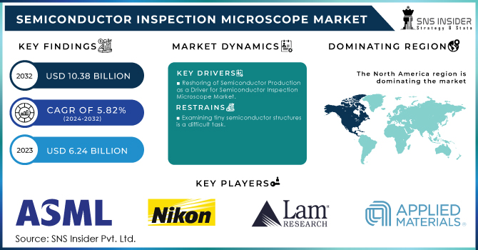
The Semiconductor Inspection Microscope Market size was valued at USD 6.98 billion in 2025E and is expected to Reach USD 10.98 billion by 2033 and grow at a CAGR of 5.82% over the forecast period of 2026-2033.
Get More Information on Semiconductor Inspection Microscope Market - Request Sample Report
Cities such as Columbus, Ohio, are constructing new water treatment facilities to support the increasing chip production, while locations like upstate New York are erecting water storage tanks. Having a well-thought-out water management strategy is essential for drawing in chip manufacturers and maintaining long-term sustainability in operations. Saving water is extremely important, particularly in areas prone to drought. The semiconductor industry is a major user of water, even though it is often disregarded in water conversations. Although recycling wastewater is a common practice, the treatment of contaminated water from chip manufacturing is difficult. Creative methods such as custom reverse osmosis techniques are being created to tackle this issue. Responsible water management will become more crucial as the semiconductor industry grows worldwide, in order to promote sustainable development and reduce environmental harm.
Semiconductor Inspection Microscope Market Size and Forecast:
-
Market Size in 2025E: USD 6.98 Billion
-
Market Size by 2033: USD 10.98 Billion
-
CAGR: 5.82% from 2026 to 2033
-
Base Year: 2025E
-
Forecast Period: 2026–2033
-
Historical Data: 2022–2024
Semiconductor Inspection Microscope Market Highlights:
-
Reshoring of semiconductor production, supported by the CHIPS and Science Act, is driving demand for advanced inspection microscopes in the U.S.
-
Significant funding (USD 6.6 billion to TSMC and additional support for Intel and Samsung) is accelerating domestic chip manufacturing and associated equipment needs.
-
The CHIPS Act encourages domestic production of semiconductor inspection equipment, fostering self-reliant supply chains and local innovation.
-
Inspecting nanoscale semiconductor structures remains challenging; conventional optical microscopes are limited by diffraction, requiring high-resolution and efficient SEM/TEM tools.
-
National initiatives like the National Semiconductor Technology Center (NSTC) and National Advanced Packaging Manufacturing Program (NAPMP) aim to boost electronics manufacturing innovation and collaboration.
-
Advanced microscopy technologies—including AI-driven analysis, expansion microscopy, and time-resolved electron microscopy—enable defect detection at sub-200 nm (SEM) and sub-50 pm (TEM), enhancing inspection precision and throughput.
Semiconductor Inspection Microscope Market Drivers:
-
Reshoring of Semiconductor Production as a Driver for Semiconductor Inspection Microscope Market
The market for semiconductor inspection microscope is on the rise. This is due to the fact that chip producers must continuously create components that are smaller and more advanced. With the increasing need for top-notch chips, the market is predicted to continue its growth. The semiconductor industry reached a significant milestone with the USD 6.6 billion grant given to TSMC through the CHIPS and Science Act. This investment, along with funds for Intel and Samsung, shows a move towards bringing chip manufacturing back to the U.S. Geopolitical tensions and the need for strong supply chains are driving this trend, which is a significant factor for the Semiconductor Inspection Microscope market.
As domestic chip production increases, there will be a growing need for advanced inspection equipment. The push to produce cutting-edge chips like TSMC's upcoming 2nm nodes requires tighter quality control steps. Semiconductor inspection microscope are essential tools in environments where detecting tiny defects at Nano scale levels is crucial. Moreover, the growth in local manufacturing will encourage the development of a strong network of related businesses, such as suppliers of equipment and providers of services, which will in turn boost the need for inspection microscope. This shift in semiconductor manufacturing approach is anticipated to create a significant growth potential for the Semiconductor Inspection Microscope market.
-
Chips Act and Domestic Semiconductor Equipment Production Growth beyond Chips
The main goal of the CHIPS and Science Act of 2023 is to not only increase chip production, but also to rejuvenate the overall electronics manufacturing industry in the United States. Although the focus is primarily on funding for chip fabrication, the act also plays a vital role in supporting domestic semiconductor equipment manufacturing, which is often overlooked. The emphasis on manufacturing equipment will have a major effect on the Semiconductor Inspection Microscope industry. The CHIPS Act acknowledges that specialized equipment, such as inspection microscopes, plays a crucial role in chip manufacturing. At present, a substantial amount of this equipment is obtained from foreign countries. The goal of the act is to establish a self-sustaining domestic supply chain by encouraging the production of semiconductor equipment within the country through funding opportunities such as the USD 500 million CHIPS Program Office FOA. This change will lead to an increase in the need for Semiconductor Inspection Microscope produced within the country. With the increase in output from domestic chip manufacturing plants, there will be a higher demand for inspection microscope sourced locally. The close relationship between chipmakers and equipment manufacturers promotes quicker lead times, better communication, and swifter troubleshooting, which are essential for efficient production. The emphasis of the CHIPS Act on promoting creativity in the US semiconductor sector is expected to result in the creation of advanced inspection microscope designed to meet the unique requirements of American chip manufacturers. This indigenous innovation environment will additionally encourage the utilization of inspection equipment made locally. In summary, the emphasis on domestic semiconductor equipment manufacturing in the CHIPS Act serves as a strong catalyst for the growth of the Semiconductor Inspection Microscope market. By promoting a self-reliant supply chain and fostering domestic innovation, the law sets the United States up to lead in both chip manufacturing and the essential equipment needed for it.
Semiconductor Inspection Microscope Market Restraints:
-
Examining tiny semiconductor structures is a difficult task.
Conventional optical microscopes face restrictions due to light diffraction, which makes it difficult to detect features smaller than 200 nanometers. The complexity of modern chips, with their intricate 3D structures, further complicates defect detection. Achieving a balance between high-resolution inspection and quick throughput is essential for effective manufacturing, but reaching this balance is still a major challenge. While inspecting a wafer may only take seconds, analyzing it with SEM can take minutes, affecting production efficiency.
Semiconductor Inspection Microscope Market Opportunities:
-
Establishing a National Hub for Innovation in Electronics Manufacturing
ASIC's goal is to establish a nationwide network dedicated to revitalizing the electronics manufacturing sector in the United States. This platform will serve as an adaptable area for research, innovation, and sharing of technology, fostering collaboration between industry, academia, and government. ASIC is recommending the establishment of a National Semiconductor Technology Center (NSTC) and a National Advanced Packaging Manufacturing Program (NAPMP) as vital components of this ecosystem. ASIC aims to accelerate innovation, enhance supply chain resilience, and uphold America's leadership in semiconductor technology by uniting different stakeholders in the electronics supply chain. If this ambitious project is successful, it could jumpstart the growth of a semiconductor industry that is more scalable, long-lasting, and focused on local needs.
-
Innovations in microscopy are transforming the way semiconductor inspection is done.
The growing requirement for precise and efficient examination has escalated with the increasing need for semiconductors in various industries. Modern microscopes have advanced features like better image quality, faster inspection rates, and automated analysis to address these difficulties. AI and machine learning enhance the inspection process by enabling quicker identification of defects and improving efficiency. Recent advancements, such as expansion microscopy and time-resolved electron microscopy, have extended the limits of resolution. Expansion microscopy surpasses the light diffraction limit, allowing for sub-200 nm structures to be seen, and time-resolved electron microscopy uses electrons' shorter wavelengths to achieve magnifications of up to 2 million iterations in Scanning Electron Microscopy (SEM) and 50 million iterations in Transmission Electron Microscopy (TEM) yield resolutions of approximately 0.5 nm in SEM and less than 50 pm in TEM. These technological developments are transforming semiconductor inspection, allowing for greater understanding of material characteristics and defect examination.
Semiconductor Inspection Microscope Market Segment Analysis:
By Type
In 2025, the Electron Microscope had a 35% market share in the Semiconductor Inspection Microscope Market. The electron microscopes, specifically Scanning Electron Microscopes (SEMs), are commonly utilized in semiconductor examination due to their high resolution and capability to visualize both the exterior and interior features of semiconductor devices. Among all microscope types, electron microscopes were the top revenue generator, as they provide precise images of semiconductor devices essential for quality control and reliability assurance. They provide solutions with a precision of just a few nanometers, perfect for detecting small flaws and examining the intricate features of semiconductor parts. The SU5000 SEM from Hitachi offers excellent imaging quality and a wide range of analysis options, making it a top pick for semiconductor inspection. Transmission Electron Microscopes (TEMs) are employed for specialized tasks, such as observing the crystal structure of semiconductor materials. Detailed images of the internal structure at the atomic level are offered by TEMs, which can achieve resolutions even higher than SEMs, usually below 1 nanometer, enabling the study of material's internal structure and defects at the atomic level. Provides automated features and user-friendly interfaces, improving efficiency in high-volume settings. The Helios 5 UX Dual Beam by Thermo Fisher is a blend of SEM and Focused Ion Beam (FIB) technologies. Provides precise imaging and thorough material analysis.
By Components
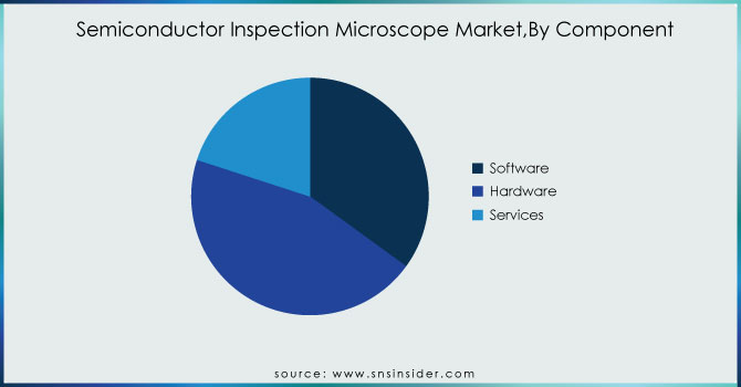
Based on Component, Hardware dominated the Semiconductor Inspection Microscope Market with 45% of share in 2025. The microscope hardware, such as the optical system, illumination system, and stage, controls the market because of its high cost and complexity. Creating and producing the hardware requires a significant amount of skill and knowledge. The optical system, which is the core component of a microscope, magnifies small semiconductor structures to enable accurate inspection. Nikon's line of Eclipse microscopes utilizes sophisticated optics to offer high-quality imaging that is essential for inspecting semiconductors. The lighting system supplies the required illumination to improve the visibility of the semiconductor structures. Carl Zeiss' Axio Imager series includes advanced lighting systems that enable a variety of inspection techniques, providing versatility for different semiconductor inspection jobs.
Get Customized Report as per Your Business Requirement - Request For Customized Report
By Application
The Semiconductor Inspection Microscope Market is segmented by application, including Integrated Circuits, Transistors, Memory Blocks, Interconnection Devices, and Others. Integrated circuits lead the market due to their growing complexity, which makes defect detection more challenging. Semiconductor inspection microscopes are crucial for examining integrated circuits for defects like scratches, cracks, and particles, ensuring they meet quality standards and perform reliably. Memory blocks are the fastest-growing application, fueled by the rising demand for memory chips.
Semiconductor Inspection Microscope Market Regional Analysis:
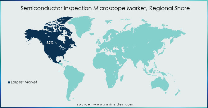
North America Semiconductor Inspection Microscope Market Trends:
North America is witnessing growing adoption of semiconductor inspection microscopes driven by increasing use of AI and machine learning to detect defects with greater precision. The presence of major chip manufacturers and advanced research institutions is boosting demand for ultra-high-resolution inspection systems. Innovations in advanced packaging and chiplet architectures are further requiring precise inspection capabilities. Additionally, the CHIPS and Science Act is accelerating local semiconductor production and increasing investments in inspection technologies, while rising cybersecurity concerns around chip authentication are enhancing the focus on secure inspection tools.
Asia-Pacific Semiconductor Inspection Microscope Market Trends:
Asia-Pacific continues to dominate the market due to rapid semiconductor manufacturing expansion in China, Taiwan, South Korea, and Japan. Growing investments in EUV lithography and advanced nodes are pushing demand for extremely accurate inspection microscopes. The increasing production of EVs, IoT devices, smartphones, and consumer electronics is driving the need for superior defect detection tools. Government subsidies and semiconductor stimulus programs are accelerating fabs and inspection infrastructure growth, while automation and AI-driven defect analytics are improving yield, speed, and inspection efficiency across the region.
Europe Semiconductor Inspection Microscope Market Trends:
Europe’s semiconductor inspection microscope market is expanding due to strict EU quality standards and increasing adoption of precision engineering solutions. The EU Chips Act is driving localized chip production and stimulating demand for advanced inspection tools. With rising demand for automotive semiconductors, manufacturers are focusing on high-reliability defect detection. Research partnerships between universities, technology labs, and industrial manufacturers are accelerating microscopy innovation for nano-fabrication and metrology, solidifying Europe’s position as a technology-focused semiconductor inspection hub.
Latin America Semiconductor Inspection Microscope Market Trends:
Latin America is experiencing gradual growth in semiconductor inspection microscopes as electronics assembly, consumer device manufacturing, and automotive chip testing expand in countries like Brazil and Mexico. Industrial automation and smart manufacturing trends are increasing the need for precision quality control tools. University and government collaboration with global semiconductor companies is steadily enhancing regional microelectronics expertise. Incentives to boost local electronics production and increasing PCB packaging and testing activities are further contributing to the demand for high-accuracy inspection systems.
Middle East & Africa Semiconductor Inspection Microscope Market Trends:
The Middle East & Africa (MEA) region is developing as a potential market as countries such as UAE, Saudi Arabia, and South Africa invest in semiconductor research, nano-technology centers, and advanced electronics production. Growing initiatives in AI, robotics, smart city development, and 5G deployment are pushing demand for semiconductor inspection microscopes. Partnerships with international semiconductor firms are building local knowledge and laboratory capabilities. Although still in early stages, expanding chip testing and research infrastructure is creating long-term growth opportunities for inspection technology adoption across the region.
Semiconductor Inspection Microscope Market Key Players:
-
ASML Holdings HV,
-
Nikon Corporation
-
Lam Research Corporation
-
Tokyo Electron Limited
-
Takano Co., Ltd.
-
Onto Innovation, Inc.
-
Toray Engineering
-
Hitachi Group
-
Canon Inc.
-
JEOL Ltd.
-
Ultratech (acquired by Veeco Instruments)
-
Rudolph Technologies
-
Advantest Corporation
-
FEI Company (part of Thermo Fisher Scientific)
-
Zeiss Group
-
Rigaku Corporation
-
Bruker Corporation
-
Mitutoyo Corporation
Semiconductor Inspection Microscope Market Competitive Landscape:
KLA Corporation (Established in 1975) is a global leader in semiconductor process control and yield management solutions. The company provides advanced inspection, metrology, and analytics technologies that enable precise defect detection and manufacturing optimization for chips, displays, and electronics, supporting innovation in AI, consumer electronics, automotive, and advanced computing markets.
-
In Sep 2025 – KLA Corporation launched new AI-centric semiconductor process-control solutions enabling nanoscale defect detection for advanced GPU, HBM, and heterogeneous chip architectures to support next-generation AI manufacturing.
Onto Innovation Inc., established in 2019 through the merger of Nanometrics and Rudolph Technologies, is a leading provider of semiconductor process control, metrology, and inspection solutions. The company delivers advanced technologies for logic, memory, advanced packaging, and specialty devices, helping manufacturers improve yield, reliability, and production efficiency globally.
-
In September 2025, Onto Innovation Showcases Advanced Metrology & Inspection Solutions at SEMICON West 2025, Driving Leadership in AI and Next-Gen Semiconductor Packaging
| Report Attributes | Details |
|---|---|
| Market Size in 2025E | USD 6.98 Billion |
| Market Size by 2033 | USD 10.98 Billion |
| CAGR | CAGR of 5.82% From 2026 to 2033 |
| Base Year | 2025E |
| Forecast Period | 2026-2033 |
| Historical Data | 2022-2024 |
| Report Scope & Coverage | Market Size, Segments Analysis, Competitive Landscape, Regional Analysis, DROC & SWOT Analysis, Forecast Outlook |
| Key Segments | • By Type (Electron Microscope, Scanning Probe Microscope, Optical Microscopes & Others) • By Components (Software, Hardware & Services) • By Application (Transistors, Memory Blocks, Interconnection Devices Integrated Circuits & Others) |
| Regional Analysis/Coverage | North America (US, Canada), Europe (Germany, UK, France, Italy, Spain, Russia, Poland, Rest of Europe), Asia Pacific (China, India, Japan, South Korea, Australia, ASEAN Countries, Rest of Asia Pacific), Middle East & Africa (UAE, Saudi Arabia, Qatar, South Africa, Rest of Middle East & Africa), Latin America (Brazil, Argentina, Mexico, Colombia, Rest of Latin America). |
| Company Profiles | ASML Holdings NV, Nikon Corporation, Lam Research Corporation, Applied Materials Inc., Tokyo Electron Limited, Takano Co., Ltd., KLA Corporation, Onto Innovation, Inc., Toray Engineering, Hitachi Group, Canon Inc., JEOL Ltd., Ultratech (acquired by Veeco Instruments), Rudolph Technologies, Advantest Corporation, FEI Company (part of Thermo Fisher Scientific), Zeiss Group, Rigaku Corporation, Bruker Corporation, Mitutoyo Corporation |