Semiconductor Metrology and Inspection Equipment Market Size:

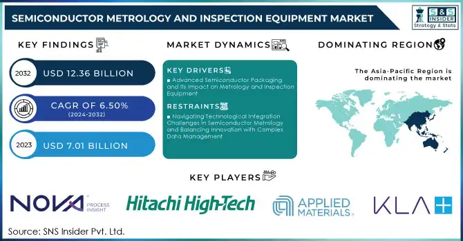
The Semiconductor Metrology and Inspection Equipment Market size was valued at USD 7.46 billion in 2024 and is expected to grow to USD 12.36 billion by 2032 and grow at a CAGR of 6.50 % over the forecast period of 2025-2032. Semiconductor metrology and inspection are integral to the semiconductor manufacturing process, which involves 400 to 600 steps and takes one to two months to complete. Any flaws detected late in the process can lead to the loss of all efforts in subsequent stages. Effective metrology and inspection are essential for ensuring a high yield and optimal quality. These procedures are implemented at critical stages of production to assess thin films, line widths, pattern defects, and other issues, minimizing costly downtime and maintaining high efficiency. The use of advanced UV light sources in semiconductor inspection is vital for reducing inspection times and improving pattern evaluation accuracy. As the semiconductor industry strives for more compact and high-performance integrated circuits, metrology becomes even more crucial.

Semiconductor Metrology and Inspection Equipment Market Revenue Analysis

Get More Information on Semiconductor Metrology and Inspection Equipment Market - Request Sample Report

Companies like TSMC, Infineon, Qualcomm, and Intel are increasing their chip production investments, driving up demand for metrology tools and services. The rise of smartphones, consumer electronics, automotive applications, and IoT devices, particularly with the advent of 5G networks, further fuels the demand for semiconductor materials. The GSMA projects that 5G mobile broadband connections will reach 1.1 billion by 2025, broadening the scope for semiconductor applications across industries. To stay competitive, semiconductor vendors are forming strategic partnerships to develop multifunctional inspection platforms. For example, k-Space Associates introduced the kSA XRF metrology tool, designed to measure thin film thickness with precision.

Key Semiconductor Metrology and Inspection Equipment Market Trends:

  • The adoption of 3D stacking and system-in-package (SiP) solutions is accelerating to overcome limitations of traditional chip designs.

  • Semiconductor metrology tools are evolving to deliver ultra-precise defect detection in complex multi-die packaging structures.

  • Automotive and 5G applications are driving higher demand for reliable, compact, and high-performance semiconductor devices.

  • Advanced packaging technologies like 2.5D and 3D integration are becoming critical for AI, IoT, and autonomous vehicle applications.

  • The industry is shifting toward high-resolution, high-speed inspection systems to ensure performance and reliability in advanced semiconductor packaging.

Semiconductor Metrology and Inspection Equipment Market Growth Drivers:

  • Advanced Semiconductor Packaging and Its Impact on Metrology and Inspection Equipment

The growing demand for advanced semiconductor packaging methods, such as 3D stacking and system-in-package (SiP) solutions, is driving the expansion of the semiconductor metrology and inspection equipment market. As the industry pushes to develop more compact and powerful devices, advanced packaging techniques play a crucial role in addressing the limits of traditional chip manufacturing. With increasing complexity in designs, particularly in automotive and 5G applications, packaging technologies such as 2.5D and 3D integration are becoming essential to meet the growing demand for smaller, faster, and more efficient semiconductor devices. These advanced packaging methods, which involve stacking multiple dies or chips to increase interconnect density and reduce signal paths, require highly specialized metrology tools. These tools must deliver ultra-precise measurements to detect defects in stacked chips, voids, or delamination at a micrometer level. In sectors like automotive, where semiconductor reliability is crucial for safety, the need for such high-resolution inspection is more important than ever. Advanced packaging offers a solution by combining multiple chips into a single package, thus addressing the limitations of traditional packaging. With applications in AI, IoT, and autonomous vehicles, the need for low-power, high-performance chips is escalating.

Semiconductor Metrology and Inspection Equipment Market Restraints:

  • Navigating Technological Integration Challenges in Semiconductor Metrology and Balancing Innovation with Complex Data Management

A major restraint in the semiconductor metrology and inspection equipment market stems from the challenges associated with integrating a range of advanced metrology tools—optical, X-ray, and electron microscopes—each with distinct calibration and data output requirements. These tools must be synchronized to ensure accurate and consistent defect detection across varying scales, but achieving this integration is complicated by the complexity of aligning different hardware, software, and operator processes. Additionally, the vast amount of data generated by these systems often overwhelms traditional processing pipelines, necessitating advanced, real-time software solutions to effectively manage and analyze the data. Without seamless integration, the risk of delays, errors, and inefficiencies increases, ultimately driving up costs and slowing down market innovation.

Semiconductor Metrology and Inspection Equipment Market Segment Analysis:

By Type

In 2024, the lithography metrology segment dominates the semiconductor metrology and inspection equipment market, of around 41% of total revenue. This leadership is due to its crucial role in supporting advanced manufacturing processes like node miniaturization and producing larger wafer sizes. Lithography metrology tools, such as Critical Dimension Scanning Electron Microscopes (CD-SEMs), ensure the precision and accuracy required for wafer patterning, essential for ultra-large-scale integrated circuits. The segment’s growth is fueled by increasing demand for high-performance semiconductor devices, particularly in AI, 5G, and consumer electronics. Major companies like ASML and KLA continue to lead the segment, pushing advancements in defect detection and mask optimization to strengthen their market position further.

Semiconductor Metrology and Inspection Equipment Market Regional Analysis:

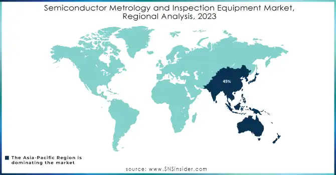
Asia Pacific Semiconductor Metrology and Inspection Equipment Market Insights

In 2024, the Asia-Pacific region held a dominant share of around 45% in the semiconductor metrology and inspection equipment market, driven by the robust growth of semiconductor manufacturing in Taiwan, South Korea, China, and Japan. Taiwan, with TSMC as a key player, has driven demand for advanced metrology tools due to investments in EUV lithography and 3D packaging. South Korea's semiconductor giants, Samsung and SK Hynix, continue to invest in next-gen technologies like DRAM and NAND flash, fueling the demand for wafer inspection and defect detection. China's push for self-reliance in semiconductor production further accelerates the need for advanced metrology systems. Japan remains a leader in precision equipment, with companies like Tokyo Electron and Nikon at the forefront. 

North America Semiconductor Metrology and Inspection Equipment Market Insights

In 2024, North America emerged as the fastest-growing region in the semiconductor metrology and inspection equipment market, driven by significant advancements in semiconductor manufacturing and technological innovation. The United States, with key players like Intel, Micron, and GlobalFoundries, has been at the forefront of expanding semiconductor operations. Intel’s investments in next-gen technologies, including advanced process nodes and 3D packaging, have boosted demand for precise metrology tools. Additionally, the U.S. government's CHIPS Act, which supports domestic semiconductor manufacturing, further accelerates growth. Micron’s advancements in memory chips and the rise of AI and 5G technologies also contribute to the region's robust demand for inspection systems. These factors position North America as a leader in semiconductor metrology, sustaining rapid growth.

Europe Semiconductor Metrology and Inspection Equipment Market Insights

The Europe semiconductor metrology and inspection equipment market is growing steadily, driven by rising demand for advanced chips in automotive, industrial automation, and 5G infrastructure. With Europe’s strong semiconductor ecosystem and focus on precision manufacturing, adoption of advanced inspection tools is increasing. Investments in R&D, particularly in Germany and the Netherlands, further accelerate technological advancements and market expansion.

Latin America (LATAM) and Middle East & Africa (MEA) Semiconductor Metrology and Inspection Equipment Market Insights

The Latin America and Middle East & Africa semiconductor metrology and inspection equipment market is emerging, supported by growing demand for electronics, automotive, and telecom applications. While semiconductor manufacturing capacity is limited, rising adoption of IoT, AI, and 5G technologies fuels equipment demand. Government initiatives and foreign investments are gradually enhancing regional capabilities, creating opportunities for metrology and inspection solutions.

Semiconductor-Metrology-and-Inspection-Equipment-Market by regional

Need Any Customization Research On Semiconductor Metrology and Inspection Equipment Market - Inquiry Now

Semiconductor Metrology and Inspection Equipment Companies are:

  • KLA Corporation

  • Applied Materials, Inc.

  • Hitachi High-Tech Corporation

  • ASML Holding N.V. 

  • Nova Measuring Instruments Ltd.

  • Nanometrics Incorporated 

  • Rudolph Technologies, Inc. 

  • Thermo Fisher Scientific Inc. 

  • Carl Zeiss AG 

  • Nikon Corporation 

  • Onto Innovation Inc. 

  • Bruker Corporation 

  • Advantest Corporation

  • SCREEN Holdings Co., Ltd. 

  • Camtek Ltd. 

  • Tokyo Electron Limited

  • Lam Research Corporation

  • ASM International N.V. 

  • Fujifilm Holdings Corporation 

  • Keysight Technologies, Inc. 

  • Qualcomm 

  • TSMC 

  • Infineon Technologies 

Competitive Landscape for Semiconductor Metrology and Inspection Equipment Market:

Hitachi High-Tech Corporation plays a vital role in the semiconductor metrology and inspection equipment market, offering advanced solutions such as scanning electron microscope (SEM)-based systems and defect review tools. The company focuses on enabling precise measurement and defect detection at nanometer scales, supporting next-generation semiconductor manufacturing. With strong R&D capabilities and global presence, Hitachi High-Tech drives innovation in process control, helping manufacturers meet the demands of miniaturization, 5G, automotive, and AI-driven applications.

  • March 14-Hitachi High-Tech launches the LS9300AD wafer surface inspection system, offering high-sensitivity detection of low-aspect microscopic defects on both front and backside wafer surfaces. Equipped with a new Differential Interference Contrast (DIC) optical system, it improves yield and reduces inspection costs by enabling high-throughput detection of shallow, irregular defects.

KLA Corporation is a global leader in semiconductor metrology and inspection equipment, providing advanced process control, yield management, and defect detection solutions. Its comprehensive portfolio includes wafer inspection, metrology, and data analytics tools that enable manufacturers to optimize production efficiency and ensure device reliability. KLA’s innovations support critical applications in advanced packaging, 5G, AI, and automotive semiconductors, making it a key player in addressing scaling challenges in next-generation chip manufacturing.

  • Nov 8, 2023, KLA Instruments expands its metrology portfolio with new systems including the Filmetrics® R54-300 for 300mm wafer sheet resistance mapping and the F54-XYT-300 and F60-c film thickness mapping systems, offering enhanced process optimization and automated, high-speed wafer measurement.

Semiconductor Metrology and Inspection Equipment Market Report Scope:

Report Attributes Details
Market Size in 2024 USD 7.46 Billion
Market Size by 2032 USD 12.36 Billion
CAGR CAGR of 6.50% From 2025 to 2032
Base Year 2024
Forecast Period 2025-2032
Historical Data 2021-2023
Report Scope & Coverage Market Size, Segments Analysis, Competitive  Landscape, Regional Analysis, DROC & SWOT Analysis, Forecast Outlook
Key Segments • By Type (Lithography Metrology, Wafer Inspection, Thin Film Metrology, Other Process Control Systems)
Regional Analysis/Coverage North America (US, Canada), Europe (Germany, France, UK, Italy, Spain, Poland, Turkey, Rest of Europe), Asia Pacific (China, India, Japan, South Korea, Singapore, Australia, Taiwan,  Rest of Asia Pacific), Middle East & Africa (UAE, Saudi Arabia, Qatar, South Africa, Rest of Middle East & Africa), Latin America (Brazil, Argentina, Rest of Latin America)
Company Profiles KLA Corporation, Applied Materials, Inc., Hitachi High-Tech Corporation, ASML Holding N.V., Nova Measuring Instruments Ltd., Nanometrics Incorporated, Rudolph Technologies, Inc., Thermo Fisher Scientific Inc., Carl Zeiss AG, Nikon Corporation, Onto Innovation Inc., Bruker Corporation, Advantest Corporation, SCREEN Holdings Co., Ltd., Camtek Ltd., Tokyo Electron Limited, Lam Research Corporation, ASM International N.V., Fujifilm Holdings Corporation, Keysight Technologies, Inc.

Table of Content

1. Introduction

1.1 Market Definition & Scope

 1.2 Research Assumptions & Abbreviations

 1.3 Research Methodology

2. Executive Summary

2.1 Market Snapshot

 2.2 Market Absolute $ Opportunity Assessment & Y-o-Y Analysis, 2021–2032

 2.3 Market Size & Forecast, By Segmentation, 2021–2032

  2.3.1 Market Size By Type

 2.4 Market Share & Bps Analysis By Region, 2024

 2.5 Industry Growth Scenarios – Conservative, Likely & Optimistic

 2.6 Industry CxO’s Perspective

3. Market Overview

3.1 Market Dynamics

  3.1.1 Drivers

  3.1.2 Restraints

  3.1.3 Opportunities

  3.1.4 Key Market Trends

 3.2 Industry PESTLE Analysis

 3.3 Key Industry Forces (Porter’s) Impacting Market Growth

 3.4 Industry Supply Chain Analysis

  3.4.1 Raw Material Suppliers

  3.4.2 Manufacturers

  3.4.3 Distributors/Suppliers

  3.4.4 Customers/End-Users

 3.5 Industry Life Cycle Assessment

 3.6 Parent Market Overview

 3.7 Market Risk Assessment

4. Statistical Insights & Trends Reporting

4.1 Pricing Analysis & Forecast

  4.1.1 Overview

  4.1.2 Pricing Analysis & Forecast By Type, 2021–2032

  4.1.3 Price Benchmarking By Key Players, 2024

 4.2 Regulatory Landscape

  4.2.1 Overview

  4.2.2 Regulatory Trends By Key Countries

  4.2.3 Regulatory Outlook By Type Type

 4.3 Trade Analysis

  4.3.1 Overview

  4.3.2 Import Analysis (Value & Volume), By Country, 2021–2024

  4.3.3 Export Analysis (Value & Volume), By Country, 2021–2024

  4.3.4 Major Importing Countries

  4.3.5 Major Exporting Countries

5. Semiconductor Metrology and Inspection Equipment Market Segmental Analysis & Forecast, By Type, 2021 – 2032, Value (USD Billion)

5.1 Introduction

 5.2 Lithography Metrology

  5.2.1 Key Trends

  5.2.2 Market Size & Forecast, 2021 – 2032

 5.3 Wafer Inspection

  5.3.1 Key Trends

  5.3.2 Market Size & Forecast, 2021 – 2032

 5.4 Thin Film Metrology

  5.4.1 Key Trends

  5.4.2 Market Size & Forecast, 2021 – 2032

 5.5 Other Process Control Systems

  5.5.1 Key Trends

  5.5.2 Market Size & Forecast, 2021 – 2032

6. Semiconductor Metrology and Inspection Equipment Market Segmental Analysis & Forecast By Region, 2021 – 2025, Value (USD Billion)

6.1 Introduction

6.2 North America

 6.2.1 Key Trends

 6.2.2 Semiconductor Metrology and Inspection Equipment Market Size & Forecast, By Type, 2021 – 2032

 6.2.3 Semiconductor Metrology and Inspection Equipment Market Size & Forecast, By Country, 2021 – 2032

  6.2.3.1 USA

   6.2.3.1.1 Semiconductor Metrology and Inspection Equipment Market Size & Forecast, By Type, 2021 – 2032

  6.2.3.2 Canada

   6.2.3.2.1 Semiconductor Metrology and Inspection Equipment Market Size & Forecast, By Type, 2021 – 2032

6.3 Europe

 6.3.1 Key Trends

 6.3.2 Semiconductor Metrology and Inspection Equipment Market Size & Forecast, By Type, 2021 – 2032

 6.3.3 Semiconductor Metrology and Inspection Equipment Market Size & Forecast, By Country, 2021 – 2032

  6.3.3.1 Germany

   6.3.3.1.1 Semiconductor Metrology and Inspection Equipment Market Size & Forecast, By Type, 2021 – 2032

  6.3.3.2 UK

   6.3.3.2.1 Semiconductor Metrology and Inspection Equipment Market Size & Forecast, By Type, 2021 – 2032

  6.3.3.3 France

   6.3.3.3.1 Semiconductor Metrology and Inspection Equipment Market Size & Forecast, By Type, 2021 – 2032

  6.3.3.4 Italy

   6.3.3.4.1 Semiconductor Metrology and Inspection Equipment Market Size & Forecast, By Type, 2021 – 2032

  6.3.3.5 Spain

   6.3.3.5.1 Semiconductor Metrology and Inspection Equipment Market Size & Forecast, By Type, 2021 – 2032

  6.3.3.6 Russia

   6.3.3.6.1 Semiconductor Metrology and Inspection Equipment Market Size & Forecast, By Type, 2021 – 2032

  6.3.3.7 Poland

   6.3.3.7.1 Semiconductor Metrology and Inspection Equipment Market Size & Forecast, By Type, 2021 – 2032

  6.3.3.8 Rest of Europe

   6.3.3.8.1 Semiconductor Metrology and Inspection Equipment Market Size & Forecast, By Type, 2021 – 2032

6.4 Asia-Pacific

 6.4.1 Key Trends

 6.4.2 Semiconductor Metrology and Inspection Equipment Market Size & Forecast, By Type, 2021 – 2032

 6.4.3 Semiconductor Metrology and Inspection Equipment Market Size & Forecast, By Country, 2021 – 2032

  6.4.3.1 China

   6.4.3.1.1 Semiconductor Metrology and Inspection Equipment Market Size & Forecast, By Type, 2021 – 2032

  6.4.3.2 India

   6.4.3.2.1 Semiconductor Metrology and Inspection Equipment Market Size & Forecast, By Type, 2021 – 2032

  6.4.3.3 Japan

   6.4.3.3.1 Semiconductor Metrology and Inspection Equipment Market Size & Forecast, By Type, 2021 – 2032

  6.4.3.4 South Korea

   6.4.3.4.1 Semiconductor Metrology and Inspection Equipment Market Size & Forecast, By Type, 2021 – 2032

  6.4.3.5 Australia

   6.4.3.5.1 Semiconductor Metrology and Inspection Equipment Market Size & Forecast, By Type, 2021 – 2032

  6.4.3.6 ASEAN Countries

   6.4.3.6.1 Semiconductor Metrology and Inspection Equipment Market Size & Forecast, By Type, 2021 – 2032

  6.4.3.7 Rest of Asia-Pacific

   6.4.3.7.1 Semiconductor Metrology and Inspection Equipment Market Size & Forecast, By Type, 2021 – 2032

6.5 Latin America

 6.5.1 Key Trends

 6.5.2 Semiconductor Metrology and Inspection Equipment Market Size & Forecast, By Type, 2021 – 2032

 6.5.3 Semiconductor Metrology and Inspection Equipment Market Size & Forecast, By Country, 2021 – 2032

  6.5.3.1 Brazil

   6.5.3.1.1 Semiconductor Metrology and Inspection Equipment Market Size & Forecast, By Type, 2021 – 2032

  6.5.3.2 Argentina

   6.5.3.2.1 Semiconductor Metrology and Inspection Equipment Market Size & Forecast, By Type, 2021 – 2032

  6.5.3.3 Mexico

   6.5.3.3.1 Semiconductor Metrology and Inspection Equipment Market Size & Forecast, By Type, 2021 – 2032

  6.5.3.4 Colombia

   6.5.3.4.1 Semiconductor Metrology and Inspection Equipment Market Size & Forecast, By Type, 2021 – 2032

  6.5.3.5 Rest of Latin America

   6.5.3.5.1 Semiconductor Metrology and Inspection Equipment Market Size & Forecast, By Type, 2021 – 2032

6.6 Middle East & Africa

 6.6.1 Key Trends

 6.6.2 Semiconductor Metrology and Inspection Equipment Market Size & Forecast, By Type, 2021 – 2032

 6.6.3 Semiconductor Metrology and Inspection Equipment Market Size & Forecast, By Country, 2021 – 2032

  6.6.3.1 UAE

   6.6.3.1.1 Semiconductor Metrology and Inspection Equipment Market Size & Forecast, By Type, 2021 – 2032

  6.6.3.2 Saudi Arabia

   6.6.3.2.1 Semiconductor Metrology and Inspection Equipment Market Size & Forecast, By Type, 2021 – 2032

  6.6.3.3 Qatar

   6.6.3.3.1 Semiconductor Metrology and Inspection Equipment Market Size & Forecast, By Type, 2021 – 2032

  6.6.3.4 Egypt

   6.6.3.4.1 Semiconductor Metrology and Inspection Equipment Market Size & Forecast, By Type, 2021 – 2032

  6.6.3.5 South Africa

   6.6.3.5.1 Semiconductor Metrology and Inspection Equipment Market Size & Forecast, By Type, 2021 – 2032

  6.6.3.6 Rest of Middle East & Africa

   6.6.3.6.1 Semiconductor Metrology and Inspection Equipment Market Size & Forecast, By Type, 2021 – 2032

7. Competitive Landscape

 7.1 Key Players' Positioning

 7.2 Competitive Developments

  7.2.1 Key Strategies Adopted (%), By Key Players, 2024

  7.2.2 Year-Wise Strategies & Development, 2021 – 2025

  7.2.3 Number Of Strategies Adopted By Key Players, 2024

 7.3 Market Share Analysis, 2024

 7.4 Product/Service & Application Benchmarking

  7.4.1 Product/Service Specifications & Features By Key Players

  7.4.2 Product/Service Heatmap By Key Players

  7.4.3 Application Heatmap By Key Players

 7.5 Industry Start-Up & Innovation Landscape

7.6 Key Company Profiles

 7.6.1 KLA Corporation

  7.6.1.1 Company Overview & Snapshot

  7.6.1.2 Product/Service Portfolio

  7.6.1.3 Key Company Financials

  7.6.1.4 SWOT Analysis

 7.6.2 Applied Materials, Inc.

  7.6.2.1 Company Overview & Snapshot

  7.6.2.2 Product/Service Portfolio

  7.6.2.3 Key Company Financials

  7.6.2.4 SWOT Analysis

 7.6.3 Hitachi High-Tech Corporation

  7.6.3.1 Company Overview & Snapshot

  7.6.3.2 Product/Service Portfolio

  7.6.3.3 Key Company Financials

  7.6.3.4 SWOT Analysis

 7.6.4 ASML Holding N.V.

  7.6.4.1 Company Overview & Snapshot

  7.6.4.2 Product/Service Portfolio

  7.6.4.3 Key Company Financials

  7.6.4.4 SWOT Analysis

 7.6.5 Nova Measuring Instruments Ltd.

  7.6.5.1 Company Overview & Snapshot

  7.6.5.2 Product/Service Portfolio

  7.6.5.3 Key Company Financials

  7.6.5.4 SWOT Analysis

 7.6.6 Nanometrics Incorporated

  7.6.6.1 Company Overview & Snapshot

  7.6.6.2 Product/Service Portfolio

  7.6.6.3 Key Company Financials

  7.6.6.4 SWOT Analysis

 7.6.7 Rudolph Technologies, Inc.

  7.6.7.1 Company Overview & Snapshot

  7.6.7.2 Product/Service Portfolio

  7.6.7.3 Key Company Financials

  7.6.7.4 SWOT Analysis

 7.6.8 Thermo Fisher Scientific Inc.

  7.6.8.1 Company Overview & Snapshot

  7.6.8.2 Product/Service Portfolio

  7.6.8.3 Key Company Financials

  7.6.8.4 SWOT Analysis

 7.6.9 Carl Zeiss AG

  7.6.9.1 Company Overview & Snapshot

  7.6.9.2 Product/Service Portfolio

  7.6.9.3 Key Company Financials

  7.6.9.4 SWOT Analysis

 7.6.10 Nikon Corporation

  7.6.10.1 Company Overview & Snapshot

  7.6.10.2 Product/Service Portfolio

  7.6.10.3 Key Company Financials

  7.6.10.4 SWOT Analysis

 7.6.11 Onto Innovation Inc.

  7.6.11.1 Company Overview & Snapshot

  7.6.11.2 Product/Service Portfolio

  7.6.11.3 Key Company Financials

  7.6.11.4 SWOT Analysis

 7.6.12 Bruker Corporation

  7.6.12.1 Company Overview & Snapshot

  7.6.12.2 Product/Service Portfolio

  7.6.12.3 Key Company Financials

  7.6.12.4 SWOT Analysis

 7.6.13 Advantest Corporation

  7.6.13.1 Company Overview & Snapshot

  7.6.13.2 Product/Service Portfolio

  7.6.13.3 Key Company Financials

  7.6.13.4 SWOT Analysis

 7.6.14 SCREEN Holdings Co., Ltd.

  7.6.14.1 Company Overview & Snapshot

  7.6.14.2 Product/Service Portfolio

  7.6.14.3 Key Company Financials

  7.6.14.4 SWOT Analysis

 7.6.15 Camtek Ltd.

  7.6.15.1 Company Overview & Snapshot

  7.6.15.2 Product/Service Portfolio

  7.6.15.3 Key Company Financials

  7.6.15.4 SWOT Analysis

 7.6.16 Tokyo Electron Limited

  7.6.16.1 Company Overview & Snapshot

  7.6.16.2 Product/Service Portfolio

  7.6.16.3 Key Company Financials

  7.6.16.4 SWOT Analysis

 7.6.17 Lam Research Corporation

  7.6.17.1 Company Overview & Snapshot

  7.6.17.2 Product/Service Portfolio

  7.6.17.3 Key Company Financials

  7.6.17.4 SWOT Analysis

 7.6.18 ASM International N.V.

  7.6.18.1 Company Overview & Snapshot

  7.6.18.2 Product/Service Portfolio

  7.6.18.3 Key Company Financials

  7.6.18.4 SWOT Analysis

 7.6.19 Fujifilm Holdings Corporation

  7.6.19.1 Company Overview & Snapshot

  7.6.19.2 Product/Service Portfolio

  7.6.19.3 Key Company Financials

  7.6.19.4 SWOT Analysis

 7.6.20 Keysight Technologies, Inc

  7.6.20.1 Company Overview & Snapshot

  7.6.20.2 Product/Service Portfolio

  7.6.20.3 Key Company Financials

  7.6.20.4 SWOT Analysis

8. Analyst Recommendations

 8.1 SNS Insider Opportunity Map

 8.2 Industry Low-Hanging Fruit Assessment

 8.3 Market Entry & Growth Strategy

 8.4 Analyst Viewpoint & Suggestions On Market Growth

9. Assumptions

10. Disclaimer

11. Appendix

 11.1 List Of Tables

 11.2 List Of Figures

Key Segments:

By Type

  • Lithography Metrology

      • Overlay

      • Dimension Equipment

      • Mask Inspection and Metrology

  • Wafer Inspection

  • Thin Film Metrology

  • Other Process Control Systems

Request for Segment Customization as per your Business Requirement: Segment Customization Request

REGIONAL COVERAGE:

North America

  • US

  • Canada

  • Mexico

Europe

  • Eastern Europe

    • Poland

    • Romania

    • Hungary

    • Turkey

    • Rest of Eastern Europe

  • Western Europe

    • Germany

    • France

    • UK

    • Italy

    • Spain

    • Netherlands

    • Switzerland

    • Austria

    • Rest of Western Europe

Asia-Pacific

  • China

  • India

  • Japan

  • South Korea

  • Vietnam

  • Singapore

  • Australia

  • Rest of Asia Pacific

Middle East & Africa

  • Middle East

    • UAE

    • Egypt

    • Saudi Arabia

    • Qatar

    • Rest of the Middle East

  • Africa

    • Nigeria

    • South Africa

    • Rest of Africa

Latin America

  • Brazil

  • Argentina

  • Colombia

  • Rest of Latin America

Request for Country Level Research Report: Country Level Customization Request

Available Customization

With the given market data, SNS Insider offers customization as per the company’s specific needs. The following customization options are available for the report:

  • Product Analysis

  • Criss-Cross segment analysis (e.g. Product X Application)

  • Product Matrix which gives a detailed comparison of the product portfolio of each company

  • Geographic Analysis

  • Additional countries in any of the regions

  • Company Information

  • Detailed analysis and profiling of additional market players (Up to five)

An accurate research report requires proper strategizing as well as implementation. There are multiple factors involved in the completion of good and accurate research report and selecting the best methodology to compete the research is the toughest part. Since the research reports we provide play a crucial role in any company’s decision-making process, therefore we at SNS Insider always believe that we should choose the best method which gives us results closer to reality. This allows us to reach at a stage wherein we can provide our clients best and accurate investment to output ratio.

Each report that we prepare takes a timeframe of 350-400 business hours for production. Starting from the selection of titles through a couple of in-depth brain storming session to the final QC process before uploading our titles on our website we dedicate around 350 working hours. The titles are selected based on their current market cap and the foreseen CAGR and growth.


The 5 steps process:

Step 1: Secondary Research:

Secondary Research or Desk Research is as the name suggests is a research process wherein, we collect data through the readily available information. In this process we use various paid and unpaid databases which our team has access to and gather data through the same. This includes examining of listed companies’ annual reports, Journals, SEC filling etc. Apart from this our team has access to various associations across the globe across different industries. Lastly, we have exchange relationships with various university as well as individual libraries.

Secondary Research

Step 2: Primary Research

When we talk about primary research, it is a type of study in which the researchers collect relevant data samples directly, rather than relying on previously collected data.  This type of research is focused on gaining content specific facts that can be sued to solve specific problems. Since the collected data is fresh and first hand therefore it makes the study more accurate and genuine.

We at SNS Insider have divided Primary Research into 2 parts.

Part 1 wherein we interview the KOLs of major players as well as the upcoming ones across various geographic regions. This allows us to have their view over the market scenario and acts as an important tool to come closer to the accurate market numbers. As many as 45 paid and unpaid primary interviews are taken from both the demand and supply side of the industry to make sure we land at an accurate judgement and analysis of the market.

This step involves the triangulation of data wherein our team analyses the interview transcripts, online survey responses and observation of on filed participants. The below mentioned chart should give a better understanding of the part 1 of the primary interview.

Primary Research

Part 2: In this part of primary research the data collected via secondary research and the part 1 of the primary research is validated with the interviews from individual consultants and subject matter experts.

Consultants are those set of people who have at least 12 years of experience and expertise within the industry whereas Subject Matter Experts are those with at least 15 years of experience behind their back within the same space. The data with the help of two main processes i.e., FGDs (Focused Group Discussions) and IDs (Individual Discussions). This gives us a 3rd party nonbiased primary view of the market scenario making it a more dependable one while collation of the data pointers.

Step 3: Data Bank Validation

Once all the information is collected via primary and secondary sources, we run that information for data validation. At our intelligence centre our research heads track a lot of information related to the market which includes the quarterly reports, the daily stock prices, and other relevant information. Our data bank server gets updated every fortnight and that is how the information which we collected using our primary and secondary information is revalidated in real time.

Data Bank Validation

Step 4: QA/QC Process

After all the data collection and validation our team does a final level of quality check and quality assurance to get rid of any unwanted or undesired mistakes. This might include but not limited to getting rid of the any typos, duplication of numbers or missing of any important information. The people involved in this process include technical content writers, research heads and graphics people. Once this process is completed the title gets uploader on our platform for our clients to read it.

Step 5: Final QC/QA Process:

This is the last process and comes when the client has ordered the study. In this process a final QA/QC is done before the study is emailed to the client. Since we believe in giving our clients a good experience of our research studies, therefore, to make sure that we do not lack at our end in any way humanly possible we do a final round of quality check and then dispatch the study to the client.