Semiconductor Wafers Market Report Scope Overview:
The Semiconductor Wafer Market was valued at USD 17.57 billion in 2023 and is expected to reach USD 26.73 billion by 2032, growing at a CAGR of 4.80% over the forecast period 2025-2032.
Get more information on Semiconductor Wafers Market - Request Sample Report
The demand for high-performance semiconductor chips from electronics like smartphones, tablets, and laptops is one of the main driving factors. The shift towards a more connected ecosystem reliant on big data has created a demand for faster, more efficient devices, thus driving the need for advanced wafers, mainly larger diameter wafers such as 300 mm wafers and 450 mm wafers. The advent of 5G, artificial intelligence (AI), and the Internet of Things (IoT) need further efforts to solve semiconductor supply issues, which is why innovations in wafer manufacturing have become necessary for even more complex applications in communications, computing, and consumer electronics. Wafer size is expected to contribute about 70% of the global wafer output in 2024 at 300mm, with 450mm wafers still at the R&D stage. TSMC is expected to make more than 14 million 300mm wafers a month, while Samsung Electronics is preparing to increase capacity by 15% in Pyeongtaek. This will allow for the use of more than 400 EUV lithography machines by 2024 for 5nm and 3nm chip fabrication. In addition, with 5G deployment driving new demand for high-speed data transmission, silicon photonics wafer production is projected to climb by 12%.
Moreover, the adoption of electric vehicles (EV), autonomous driving technologies, and smart manufacturing have been driving up semiconductor demand. These industries demand high-performance semiconductors for power management (i.e. power modules), sensor technologies, as well as high-performance computing systems (i.e. AR and VR-based systems), and depend on advanced semiconductor wafers to meet these demands. With the continuous evolution of wafer size, material composition, and production methods, the demand for semiconductor wafers is expected to continuously grow with companies pushing the development of cutting-edge technologies across multiple industries. More industries are having Semiconductors and they increased their dependency on it and it is guaranteed that the market will grow. Over 20 million units in global EV production in 2024, causing a subsequent increase of more than 40% in semiconductor demand across the automotive industry. This demand is compounded by the growth forecasted for IoT devices, which are predicted to reach up to 30 billion by 2025. Furthermore, the global rollout of 5G networks will need 10x more semiconductors per base station by 2025.
Market Dynamics
Key Drivers:
-
Cloud Computing and Data Center Growth Drive Surge in Semiconductor Demand for Advanced Technologies
The cloud computing explosion and the growth of the data center have increased the need for semiconductor wafers across the globe. High-end processors and memory chips are the backbone of data centers, which consume insane amounts of data. The proliferation of cloud-based apps compels businesses and consumers to order out increasing orders of more capable and efficient semiconductors. The demand is underpinned by the need for the advanced semiconductor components needed By Products such as artificial intelligence (AI), big data analytics, and real-time data processing. High-speed data transmission requirements for data centers also demand more advanced wafer technology. As streaming, e-commerce, and social networking increasingly rely on cloud infrastructure, the persistent demand for semiconductors is one of the most generator market drivers. It is estimated that 90% of applications in an enterprise will be cloud-based and AI models including GPT-4 take as much as hundreds of terabytes of memory and up to 10,000 GPU cores. Test of DRAM and NAND memory demand 25%, 5G data centers are expected to carry up to 10 terabits per second of bandwidth. Moreover, data centers are expected to use more than 2% of the world's electricity demand in 2024, making it imperative for semiconductor technology to become more energy efficient.
-
Growing Demand for Energy Efficient and Sustainable Semiconductor Technologies Driving Innovation in Key Industries
The major driver is the demand for energy-efficient and sustainable technologies. With growing environmental apprehension, industries are focusing primarily on energy-efficient semiconductor devices to minimize power consumption along with environmental footprint. In addition to its significant uses for semiconductor wafers in technologies that generate and use power including renewable energy systems, smart grids, and electric vehicles. The shift towards greener technology, like low-power chips in mobile devices, smart devices, and electric vehicles is driving more wafers that are more carbon-neutral and offer more efficiency. It is supported by an emphasis on sustainability, which not only finds its roots in global regulatory pressures but also caters to the increasing demand from consumers for sustainable solutions. And, the wafer market continues to benefit from diversification into new semiconductor technologies that promote energy efficiency. Electric vehicles (EVs) are predicted to require 3-5 times more semiconductors than conventional vehicles by 2024. Power semiconductors demand in smart grids and solar inverters has grown 20--30% per year Global solar installations are expected to exceed 1,100 GW by 2024. IoT chips will still use up to 50% less energy than the last generation of low-power chips. The smart grid scenario will dominate the semiconductor market in 2025, with more than 2 million semiconductor components required for each smart grid.
Restrain:
-
Challenges in Semiconductor Wafer Production Complex Manufacturing Processes and Supply Chain Vulnerabilities Impacting Growth
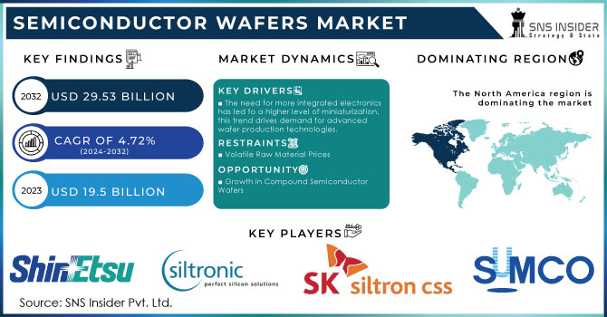
One of the key constraints in the semiconductor wafer market is the manufacturing complexity. Semiconductor wafer production includes very advanced, and high-precision processes that need dedicated equipment and high skilled workforce. Even minor differences in quality at the micro or nano scale can result in defects in the final product, which in turn constrain yield and affect overall performance. These involve a complex manufacturing process that is both time-consuming and technically challenging, thus reducing the scope for rapid scaling up to fulfill surging demand. On top of that, supply chain disruptions can be another pain point. Semiconductor wafer manufacturing requires a continuous supply of raw materials including silicon and other rare metal. Disruptions in the supply of these materials from geopolitical tensions to trade barriers to natural disasters can delay production schedules and create shortages. Due to the nature of the semiconductor supply chain, these vulnerabilities are highly susceptible to external factors impacting their availability as well as delivery of wafers to the industries dependent upon them.
Segment Analysis
By Diameter
The 150–200 mm wafer segment led the market with a 46% share in 2023, as these wafers are primarily used in conventional technologies and are cost-effective. Predominantly for mature semiconductor nodes including automotive, industrial, and consumer electronics, these wafers are intended. Support for legacy and mid-tier technologies makes them an ideal candidate to power devices that do not need the newest, highest-performing chips like some sensors, microcontrollers, and power management. This is one of the reasons why they dominate the market 150-200 mm wafers can easily be used in various applications owing to the existing manufacturing infrastructure.
300 mm wafers and above (450 mm), which are popular due to the requirement of advanced semiconductor technologies for high-performance applications are estimated to witness the highest growth over the CAGR from 2024-2032. With industries transitioning into emerging technology from AI, 5G, and high-performance computing, larger wafers mean factories can more efficiently produce high-density, high-performance chips. This enables more chips per wafer, allowing for lower costs per chip as well as increased wafer throughput. With the global demand for these advanced technologies, we shall see a considerable increase in 300 mm and 450 mm wafer utilization leading to a higher growth rate in this segment. The continuing advancements in production technology for these wafers are making 450 mm wafers all the more feasible and thus less than less-than-desirable wafers will only become more and more popular over the next few years.
By Product
The memory segment accounted for a larger share of the market in 2023 at 39.4% as the rising demand for high-capacity storage solutions across consumer data centers, and automotive industries drives the growth. On the other hand, with the exponential expansion of demand for DRAM and NAND flash and, the growing need for larger and faster memory for applications such as cloud computing, entertainment, artificial intelligence, and big data analytics, this explains a large part of the memory storage boom as well. Smartphones, laptops, more smart devices, and larger data centers demand more memory than ever before. Such memory chips are crucial, enabling a seamless combination of real-time processing and enormous amounts of data storage and pushing their market dominance even further.
Logic products are anticipated to register the fastest CAGR from 2024-2032 owing to the rapid development of semiconductor processing technologies and the growing demand for high-performance chips within emerging technologies. 5G, artificial intelligence (AI), Internet-of-Things (IoT), and autonomous vehicles call for highly advanced logic chips that need to perform complex computational tasks along with large-scale data processing. Logic chips for neuromorphic and quantum approaches Microprocessors and application-specific integrated circuits (ASICs) serve as the workhorse driving performance in next-generation devices and systems. An even more powerful logic chip landscape is speeding up with the expansion of cloud infrastructure and the emergence of more edge computing and is expected to grow faster than memory technologies during this time.
By Application
Consumer electronics accounted for 40.5% of the semiconductor wafer market in 2023 as the prominent market share holder owing to the mass penetration of smartphones, laptops, tablets, and wearable devices, among others. Because consumer electronics will keep developing over the years, demand for fast and efficient semiconductor chips (like processors, memory chips, sensors, etc.) has increased. Connected devices, thanks to the Internet of Things (IoT), are more appealing these days and add to the growing popularity of smart homes and smart wearables, and the semiconductor demand is enormous. Furthermore, we reap the additional rewards of ongoing innovation in display technologies, battery life, and user interface systems, spurred by the advancement of semiconductors, in consumer electronics.
Telecommunication is projected to expand at the highest CAGR over 2024-2032, due to the deployment of 5G networks worldwide. Telecommunications is also a critical industry that relies on advanced semiconductors to construct high-speed network infrastructure in base stations, routers, and communication chips. With 5G and beyond, the need for faster and more efficient chips to power the new-generation networks will become massive. Lastly, edge computing, along with more 5G-enabled devices and high-bandwidth applications (including augmented and virtual reality and self-driving cars) will lead to sharply increased demand for semiconductors designed for telecom networks. The swift expansion of the telecommunication infrastructure is anticipated to lead to a steep rise in semiconductor wafer usage, particularly logic and memory devices, which are integral to the transmission of high-speed data and its processing.
Need any customization research on Semiconductor Wafers Market - Enquiry Now
Regional Analysis
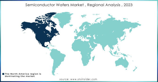
North America held the largest share of this market at 33.3% in 2023 owing to a well-developed semiconductor manufacturing industry and substantial research and development (R&D) investment. Several pivotal firms, including Intel, Qualcomm, and Micron Technology, have a strong presence in the area where advanced chips for AI, data centers, and 5G are manufactured. North America also has further assistance from government support including the U.S. CHIPS Act which allocated financial resources to strengthen the domestic semiconductor industry and lessen dependence on foreign supply chains. Microsoft also benefits from its collaborations in the new on-chip architecture for AI. If things like Intel's new advanced semiconductor fabrication facilities in Arizona are any indications, the region is leading the way in the greater and greater market creation surrounding AI.
Asia Pacific will exhibit the fastest CAGR between 2024-2032 because the region is the global center of semiconductor fab and assembly. China, South Korea, Taiwan, and Japan represent the top metro areas globally for wafer production, benefiting from high-tech virtually vertical manufacturing extended supply chains, favorable low-cost production infrastructure, and a capable skilled labor force. For illustration TSMC (Taiwan Semiconductor Manufacturing Company), Samsung Electronics (South Korea), SMIC (China), etc. are exemplary firms driving the regional development. Growing adoption of electric vehicles (EV) and consumer electronics across the Asia Pacific region and high investments in enabling 5G infrastructure and artificial intelligence (AI) technology are also boosting demand for semiconductor wafers. This is despite the region’s focus on advanced semiconductor targeting Example: TSMC to ramp up 3 nm wafers.
Key players
Some of the major players in the Semiconductor Wafer Market are:
-
Taiwan Semiconductor Manufacturing Company (TSMC) (3nm Chips, 5nm Chips)
-
Samsung Electronics (Exynos Processors, DDR4 Memory)
-
Intel Corporation (Core i7 Processors, Xeon Processors)
-
GlobalFoundries (22FDX Platform, 12LP+ Platform)
-
United Microelectronics Corporation (UMC) (28nm High-K/Metal Gate Technology, 14nm FinFET Technology)
-
Semiconductor Manufacturing International Corporation (SMIC) (14nm FinFET Process, 28nm PolySiON Process)
-
Texas Instruments (Sitara Processors, MSP430 Microcontrollers)
-
STMicroelectronics (STM32 Microcontrollers, MEMS Sensors)
-
Micron Technology (GDDR6 Memory, 3D NAND Flash)
-
SK Hynix (HBM2E Memory, LPDDR5 Memory)
-
Toshiba Corporation (BiCS Flash, ARM-based Microcontrollers)
-
ON Semiconductor (Image Sensors, Power Management ICs)
-
NXP Semiconductors (i.MX Processors, Kinetis Microcontrollers)
-
Renesas Electronics (RX Microcontrollers, RZ Microprocessors)
-
Infineon Technologies (AURIX Microcontrollers, CoolMOS Power Transistors)
-
Broadcom Inc. (Broadcom Wi-Fi Chipsets, Ethernet Switches)
-
Analog Devices (ADSP Processors, MEMS Accelerometers)
-
Applied Materials (Endura Platform, Centura Platform)
-
Lam Research (Kiyo Process Module, Flex Process Module)
-
ASML Holding (TWINSCAN NXE:3600D, TWINSCAN NXT:1950i)
Some of the Raw Material Suppliers for companies:
-
The Quartz Corp.
-
Sibelco
-
Entegris, Inc.
-
Sanritsu Chemicals Co., Ltd.
-
Resonac Corporation
-
Poco Graphite, Inc.
-
ATMI, Inc.
-
Sumco Corporation
-
Shin-Etsu Chemical Co., Ltd.
-
Siltronic AG
Recent Trends
-
In November 2024, Samsung Electronics inaugurated its new semiconductor R&D hub, NRD-K, at Giheung, South Korea, with plans to invest USD 14.8 billion by 2030 to accelerate next-gen chip innovations. The facility will focus on cutting-edge technologies like 3D DRAM and V-NAND.
-
In January 2024, Intel and UMC announced a collaboration to develop a 12-nanometer process platform, leveraging Intel's Arizona fab and UMC's foundry expertise, with production set to begin in 2027.
-
In January 2025, GlobalFoundries announced the launch of its Advanced Packaging and Photonics Center in New York, with a USD 575 million investment to enhance U.S. semiconductor manufacturing and innovation. The center will focus on advanced packaging and silicon photonics for AI, defense, and communications sectors.
| Report Attributes | Details |
|---|---|
| Market Size in 2023 | USD 17.57 Billion |
| Market Size by 2032 | USD 26.73 Billion |
| CAGR | CAGR of 4.80% From 2024 to 2032 |
| Base Year | 2023 |
| Forecast Period | 2024-2032 |
| Historical Data | 2020-2022 |
| Report Scope & Coverage | Market Size, Segments Analysis, Competitive Landscape, Regional Analysis, DROC & SWOT Analysis, Forecast Outlook |
| Key Segments | • By Diameter (Less than 150 mm, 150-200 mm, 300 mm and above (450mm,)) • By Product (Logic, Memory, Analog, Other Products) • By Application (Consumer Electronics, Industrial, Telecommunication, Automotive, Other Applications) |
| Regional Analysis/Coverage | North America (US, Canada, Mexico), Europe (Eastern Europe [Poland, Romania, Hungary, Turkey, Rest of Eastern Europe] Western Europe] Germany, France, UK, Italy, Spain, Netherlands, Switzerland, Austria, Rest of Western Europe]), Asia Pacific (China, India, Japan, South Korea, Vietnam, Singapore, Australia, Rest of Asia Pacific), Middle East & Africa (Middle East [UAE, Egypt, Saudi Arabia, Qatar, Rest of Middle East], Africa [Nigeria, South Africa, Rest of Africa], Latin America (Brazil, Argentina, Colombia, Rest of Latin America) |
| Company Profiles | Taiwan Semiconductor Manufacturing Company, Samsung Electronics, Intel Corporation, GlobalFoundries, United Microelectronics Corporation, Semiconductor Manufacturing International Corporation, Texas Instruments, STMicroelectronics, Micron Technology, SK Hynix, Toshiba Corporation, ON Semiconductor, NXP Semiconductors, Renesas Electronics, Infineon Technologies, Broadcom Inc., Analog Devices, Applied Materials, Lam Research, ASML Holding. |
| Key Drivers | • Cloud Computing and Data Center Growth Drive Surge in Semiconductor Demand for Advanced Technologies • Growing Demand for Energy Efficient and Sustainable Semiconductor Technologies Driving Innovation in Key Industries |
| RESTRAINTS | • Challenges in Semiconductor Wafer Production Complex Manufacturing Processes and Supply Chain Vulnerabilities Impacting Growth |
Frequently Asked Questions
Ans: North America dominated the Semiconductor Wafer Market in 2023.
Ans: The Consumer Electronics segment dominated the Semiconductor Wafer Market in 2023.
Ans: The major growth factor of the Semiconductor Wafer Market is the increasing demand for advanced semiconductor technologies driven by industries such as AI, 5G, and automotive electronics.
Ans: Semiconductor Wafer Market size was USD 17.57 billion in 2023 and is expected to Reach USD 26.73 billion by 2032.
Ans: The Semiconductor Wafer Market is expected to grow at a CAGR of 4.80% during 2024-2032.
Get in Touch
