Wafer Inspection System Market Size Analysis:
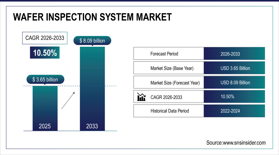
The Wafer Inspection System Market size was valued at USD 3.65 Billion in 2025E and is projected to reach USD 8.09 Billion by 2033, growing at a CAGR of 10.50% during 2026-2033.
The Wafer Inspection System Market analysis highlights the growing demand for advanced inspection tools driven by the shift toward smaller semiconductor nodes and higher yield requirements. Technological innovations such as AI, machine learning, and automation are reshaping inspection accuracy and efficiency. Rising adoption in MEMS, sensors, and advanced packaging applications further boosts market potential. Strong R&D investments, patent filings, and strategic M&A activities by leading players underline competitive intensity. Supply chain constraints and pricing dynamics continue to influence market performance.
2025: 75% systems serve 3nm/2nm production. AI automation cuts inspection time 35%. Advanced packaging demand up 45%. M&A activity doubles YoY. Component shortages ease but pricing stays 10–15% elevated.
Wafer Inspection System Market Size and Forecast:
-
Market Size in 2025: USD 3.65 Billion
-
Market Size by 2033: USD 8.09 Billion
-
CAGR: 10.50% from 2026 to 2033
-
Base Year: 2025
-
Forecast Period: 2026–2033
-
Historical Data: 2022–2024
To Get More Information On Wafer Inspection System Market - Request Free Sample Report
Wafer Inspection System Market Trends
-
Adoption of AI, machine learning, and automation enhances defect detection accuracy, enabling faster wafer inspections and reducing manufacturing costs for semiconductor fabs worldwide.
-
Rising demand for advanced nodes (7nm, 5nm, and below) fuels investments in high-precision inspection systems capable of handling ultra-fine pattern recognition.
-
Expansion of MEMS devices, sensors, and advanced packaging applications drives market growth, creating new opportunities for wafer-level inspection solutions across industries.
-
Key players increase R&D spending and patent filings in next-generation inspection technologies, fostering innovation and strengthening competitive positioning in the market.
-
Asia-Pacific leads with rapid fab expansions, while North America and Europe invest in domestic semiconductor supply chains, boosting demand for wafer inspection systems globally.
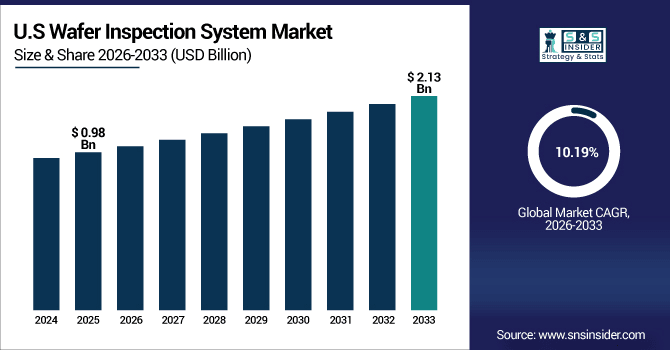
The U.S. Wafer Inspection System Market size was valued at USD 0.98 Billion in 2025E and is projected to reach USD 2.13 Billion by 2033, growing at a CAGR of 10.19% during 2026-2033. Wafer Inspection System Market growth is driven by rising investments in semiconductor manufacturing and domestic chip production under government initiatives. Strong demand for advanced nodes accelerates adoption of high-precision inspection tools. Increasing R&D spending by leading U.S. companies fosters innovation in AI and automation-enabled systems. Expanding applications in MEMS, sensors, and advanced packaging further strengthen market prospects.
Wafer Inspection System Market Growth Drivers:
-
Rising demand for advanced semiconductor nodes and precision inspection systems across global manufacturing fabs
The Wafer Inspection System Market is driven by increasing adoption of advanced semiconductor nodes such as 7nm, 5nm, and beyond. As device complexity grows, the need for ultra-precise inspection technologies to identify micro-level defects becomes critical. This trend is further fueled by rising investments in semiconductor fabrication plants worldwide, ensuring higher yield, better performance, and faster production cycles for next-generation electronics.
2025: 70% inspection tools serve 5nm/3nm nodes. Sub-3nm defect capture hits 90% accuracy. 97% target yields. $24B global fab spend fuels 40% tool adoption; cycle time down 25%.
Wafer Inspection System Market Restraints:
-
High equipment costs and complex integration challenges limit adoption for smaller fabs and emerging markets
Despite strong growth prospects, wafer inspection systems face restraints due to their high capital expenditure requirements and complex integration processes. Small and mid-sized fabs often struggle to afford advanced inspection technologies, restricting adoption beyond large players. Moreover, system maintenance, skilled labor shortages, and long installation cycles add further operational challenges, slowing market penetration in emerging economies despite rising semiconductor demand.
Wafer Inspection System Market Opportunities:
-
Expanding applications in MEMS, sensors, and advanced packaging create new growth avenues for inspection systems
Beyond traditional semiconductor wafers, wafer inspection systems are finding significant opportunities in MEMS, sensors, and advanced packaging. The proliferation of IoT devices, autonomous vehicles, and wearable electronics accelerates demand for precise inspection at wafer-level. These emerging applications not only broaden the customer base but also encourage technological innovation, enabling vendors to develop customized solutions and capture high-growth niches within the semiconductor ecosystem.
2024: MEMS/sensors drive 35% of new inspection demand. 50M+ IoT/autonomous vehicle chips inspected monthly. 45% vendors launch customized tools. Wafer-level packaging inspections grow 40%.
Wafer Inspection System Market Segment Analysis
-
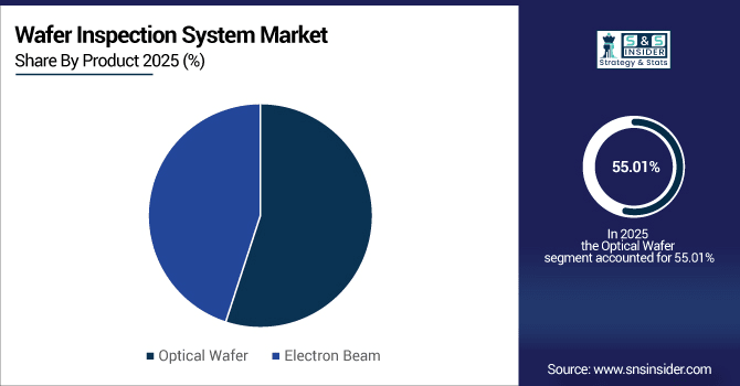
By Product, Optical Wafer inspection systems led the market with a 55.01% share. Electron Beam systems emerged as the fastest-growing product category, projected to grow at a CAGR of 8.20%.
-
By Application, Defect Detection dominated the application landscape in 2025E, accounting for 60.24% of the market. Pattern Recognition is the fastest-growing application, expected to expand at a CAGR of 9.10%.
-
By Type, Wafer Scanners held the largest market share in 2025E at 58.32%. Wafer Probers are the fastest-growing type segment, anticipated to grow at a CAGR of 7.50%.
-
By Technology, Front-End Wafer inspection commanded 62.10% market share in 2025E. Back-End Wafer inspection is the fastest-growing technology segment, projected to grow at a CAGR of 8.80%.
By Product, Optical Wafer Leads Market While Electron Beam Registers Fastest Growth
Optical wafer inspection systems currently lead the market due to their widespread adoption, cost-effectiveness, and ability to provide rapid, high-throughput defect detection across semiconductor manufacturing processes. Their efficiency makes them the preferred choice for volume production environments. However, electron beam inspection systems are registering the fastest growth as advanced nodes demand greater accuracy. With superior resolution and the ability to detect nano-level defects, electron beam tools are increasingly adopted for critical defect analysis and process monitoring.
By Application, Defect Detection Dominate While Pattern Recognition Shows Rapid Growth
Defect detection remains the dominant application segment, as semiconductor manufacturers prioritize identifying surface and sub-surface defects to improve yields and minimize manufacturing losses. The critical role of detecting even the smallest flaws ensures strong demand for inspection tools in this segment. At the same time, pattern recognition applications are showing rapid growth, supported by the increasing complexity of circuit designs. Advanced algorithms and AI-powered solutions are being deployed to identify lithography-related errors, enhancing process control and accuracy.
By Type, Wafer Scanners Lead While Wafer Probers Registers Fastest Growth
Wafer scanners lead the market due to their essential role in inspecting entire wafers with speed and precision, making them integral to high-volume semiconductor manufacturing. Their dominance is supported by continuous technological enhancements improving throughput and defect coverage. Meanwhile, wafer probers are witnessing the fastest growth. As demand for electrical testing and validation of wafers rises, especially in smaller and more complex nodes, probers provide critical data for device performance analysis, expanding their role across advanced semiconductor production.
By Technology, Front-End Wafer Lead While Back-End Wafer Grow Fastest
Front-end wafer inspection dominates the market, as it covers critical early stages of semiconductor manufacturing where precision is paramount to reduce costly downstream errors. Its dominance stems from strong demand in lithography and deposition processes. However, back-end wafer inspection technologies are growing fastest, driven by the expansion of advanced packaging, MEMS, and heterogeneous integration. These applications require specialized defect detection capabilities at later manufacturing stages, creating new growth opportunities and pushing vendors to innovate in back-end inspection solutions.
North America Wafer Inspection System Market Insights
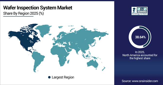
In 2025E North America dominated the Wafer Inspection System Market and accounted for 38.64% of revenue share, this leadership is due to the strong technological innovation and the presence of global semiconductor equipment leaders. Government-backed programs like the CHIPS Act drive fab expansions and local manufacturing growth. Demand is reinforced by advanced R&D in AI-driven and automation-enabled inspection tools.
Get Customized Report as Per Your Business Requirement - Enquiry Now
U.S. Wafer Inspection System Market Insights
The U.S. wafer inspection system market is driven by large-scale investments in semiconductor manufacturing and domestic chip production initiatives. Leading companies headquartered in the U.S. spearhead technological innovation in high-precision inspection.
Asia-pacific Wafer Inspection System Market Insights
Asia-pacific is expected to witness the fastest growth in the Wafer Inspection System Market over 2026-2033, with a projected CAGR of 11.26 due to its strong base of semiconductor manufacturing hubs, especially in Taiwan, South Korea, and Japan. Expanding fabrication capacity and rising investments in advanced nodes drive equipment demand. Regional players benefit from government-backed initiatives to strengthen chip independence. The presence of leading foundries ensures continuous adoption of next-gen inspection technologies.
China Wafer Inspection System Market Insights
China’s wafer inspection system market is fueled by aggressive government initiatives to build domestic semiconductor self-sufficiency. Heavy investments in fabs, packaging, and foundry expansions create strong demand for inspection tools.
Europe Wafer Inspection System Market Insights
Europe’s wafer inspection system market is supported by investments in automotive, industrial electronics, and energy-efficient semiconductors. Germany, the Netherlands, and France play leading roles in driving adoption. Regional focus on research, sustainability, and next-gen automotive chips strengthens demand. European companies are also advancing optical and electron beam technologies. Overall, Europe represents a mature yet steadily growing market for inspection systems.
Germany Wafer Inspection System Market Insights
Germany is a key driver of wafer inspection system adoption in Europe, supported by its strong automotive and industrial electronics industries. Semiconductor R&D centers and collaborations with equipment suppliers enhance local innovation. Investments in next-generation automotive semiconductors fuel demand for inspection tools.
Latin America (LATAM) and Middle East & Africa (MEA) Wafer Inspection System Market Insights
The Wafer Inspection System Market is experiencing moderate growth in the Latin America (LATAM) and Middle East & Africa (MEA) regions, due to the increasing interest in electronics manufacturing and government-led diversification strategies. Limited semiconductor infrastructure poses adoption challenges, restricting large-scale deployment. However, rising demand for consumer electronics and digitalization initiatives creates future potential. Over time, the regions are expected to serve as emerging markets for wafer inspection solutions.
Wafer Inspection System Market Competitive Landscape:
Applied Materials, Inc. is a leading player in the wafer inspection system market, offering advanced semiconductor manufacturing solutions. Its portfolio includes precision optical and e-beam inspection tools that enable defect detection at nanometer scale. Strong R&D capabilities and global presence enhance its competitive edge. Applied Materials consistently invests in next-gen technologies to support advanced node production and packaging.
-
In February 2025, Applied Materials introduced the SEMVision H20 e-beam inspection system, enhancing defect classification accuracy and throughput for advanced semiconductor nodes, accelerating yield learning and process optimization.
KLA-Tencor Corporation dominates the wafer inspection system market with its broad portfolio of optical and e-beam inspection solutions. The company is recognized for pioneering innovations in defect detection, metrology, and yield management. It serves global foundries, IDMs, and packaging companies, ensuring process control excellence.
-
In April 2025, KLA launched the 3935 and 3920 EP broadband plasma defect inspection systems, offering high sensitivity for ≤5nm logic and memory nodes, utilizing SR-DUV illumination and advanced algorithms for defect detection.
ASML Holding N.V. plays a critical role in the wafer inspection system market, primarily known for its advanced lithography equipment. It complements lithography with inspection and metrology solutions, supporting leading-edge semiconductor production. With a strong focus on EUV technology, ASML drives accuracy in defect detection and process control. Strategic collaborations further strengthen its global influence across semiconductor manufacturing ecosystems.
-
In February 2024, ASML achieved the "first light" milestone on its High NA EUV lithography system, a critical step toward enabling advanced chip production with smaller nodes, anticipated for use in Intel's 14A generation.
Pacific Technology contributes to the wafer inspection system market through its focus on innovative semiconductor inspection and metrology solutions. The company offers technologies designed for high-precision defect detection, enabling efficient semiconductor yield improvement. With growing partnerships and expanding global reach, Pacific Technology strengthens its role in niche semiconductor manufacturing markets. Its emphasis on R&D supports competitiveness in advanced nodes.
-
In March 2025, Pacific Technology unveiled its next-generation optical inspection system, incorporating AI-driven defect detection and enhanced imaging capabilities, aimed at improving yield and process control in advanced semiconductor manufacturing.
Wafer Inspection System Companies are:
-
KLA-Tencor Corporation
-
ASML Holding N.V.
-
Teradyne Inc.
-
Nanda Technologies GmbH
-
Lam Research Corporation
-
Hitachi High-Technologies Corporation
-
Hermes Microvision, Inc.
-
NXP Semiconductors
-
Synopsys
-
Onto Innovation Inc.
-
Thermo Fisher Scientific Inc.
-
JEOL Ltd.
-
Nikon Metrology NV
-
Camtek Ltd.
-
Lasertec Corporation
-
Nova Ltd.
-
SCREEN Semiconductor Solutions Co., Ltd.
-
BT Imaging Pty Ltd
| Report Attributes | Details |
|---|---|
| Market Size in 2025 | USD 3.65 Billion |
| Market Size by 2033 | USD 8.09 Billion |
| CAGR | CAGR of 10.50% From 2026 to 2033 |
| Base Year | 2025E |
| Forecast Period | 2026-2033 |
| Historical Data | 2022-2024 |
| Report Scope & Coverage | Market Size, Segments Analysis, Competitive Landscape, Regional Analysis, DROC & SWOT Analysis, Forecast Outlook |
| Key Segments | • By Product (Optical Wafer and Electron Beam) • By Application (Defect Detection and Pattern Recognition) • By Type (Wafer Scanners and Wafer Probers) • By Technology (Front-End Wafer and Back-End Wafer) |
| Regional Analysis/Coverage | North America (US, Canada), Europe (Germany, UK, France, Italy, Spain, Russia, Poland, Rest of Europe), Asia Pacific (China, India, Japan, South Korea, Australia, ASEAN Countries, Rest of Asia Pacific), Middle East & Africa (UAE, Saudi Arabia, Qatar, South Africa, Rest of Middle East & Africa), Latin America (Brazil, Argentina, Mexico, Colombia, Rest of Latin America). |
| Company Profiles | Applied Materials, Inc., KLA-Tencor Corporation, ASML Holding N.V., Pacific Technology, Teradyne Inc., Nanda Technologies GmbH, Lam Research Corporation, Hitachi High-Technologies Corporation, Hermes Microvision, Inc., NXP Semiconductors, Synopsys, Onto Innovation Inc., Thermo Fisher Scientific Inc., JEOL Ltd., Nikon Metrology NV, Camtek Ltd., Lasertec Corporation, Nova Ltd., SCREEN Semiconductor Solutions Co., Ltd., BT Imaging Pty Ltd. |
Get in Touch
