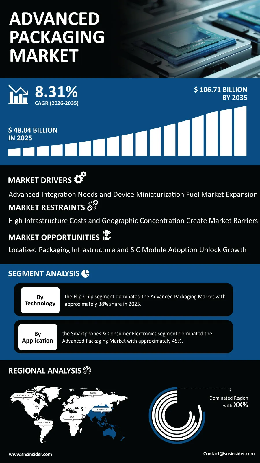
The worldwide Advanced Packaging Market is moving into an excellent expansion period due to the need for smaller and higher performing semiconductors in the areas of artificial intelligence, consumer electronics, automotive systems, and data centers. According to a recent study by SNS Insider, the global Advanced Packaging Market size valued at USD 48.04 billion in 2025, is anticipated to grow to USD 106.71 billion by 2035, registering a CAGR of 8.31% over the 2026–2035 forecast period.
The increasing intricacies in designing semiconductors have compelled the manufacturers to employ packaging techniques which consist of more than one die, memory devices, and processor in a single device. This trend has been witnessed more prominently in cases where there is a need for higher computing power without having to increase the size of the chip.
The heavy investments being made in AI infrastructure are also contributing to the increase in demand for sophisticated packaging techniques that can facilitate the incorporation of high-speed memory devices along with heavy data processing.
To Get Detailed Insights on the Advanced Packaging Market – Request a Sample Report
AI Semiconductor Demand Creates New Growth Opportunities
However, rapid growth in generative AI and computing is giving rise to business prospects for packaging companies. There is a growing need for integration of memory and computing on the same chip for AI processors, which increases the demand for packaging solutions that can offer enhanced performance and reduced communication distance.
Further, designs with multiple chiplets are becoming more common among semiconductor companies to increase their flexibility of manufacturing of chips made using varying process technologies. It helps overcome some of the design inefficiencies caused by increasing complexity of monolithic chips.
Electrification in the automotive industry is yet another opportunity area for packaging companies. Electric vehicles, ADAS chips, and power management platforms are making increased demands of semiconductors that can withstand higher heat generation and harsh conditions.
Key Market Insights Highlight Shifting Demand Patterns
Through technology, flip chip packaging is estimated to capture about 38% share of total market revenue in 2025 due to the wide application of this packaging technology in processors, communications chips, and other high-performance semiconductors. Fan-Out Wafer-Level Packaging is estimated to have the highest growth rate amongst other technologies due to demands for thin package, high integration density, and scalability in manufacture of advanced mobile and computing applications.
Consumer Electronics end-user industry is estimated to generate 48.77% of total market revenue in 2025 due to growing integration of semiconductor components in smartphones, laptops, wearable and connected devices. The automotive and EV application is estimated to experience the fastest growth due to increasing demand of semiconductors per vehicle and demands for thermal management and reliability.
Based on applications, it is estimated that smartphones and consumer electronics will capture about 45% share of the revenue in 2025. The fastest growing markets are High-Performance Computing and AI accelerators where investment in AI computing infrastructure will continue to increase from hyperscalers and tech firms.
In relation to the level of integration, 2D IC Packaging segment will remain dominant by holding about 62% of the revenue in 2025. However, 3D IC Packaging is estimated to be the fastest growing market owing to increasing adoption of stacked architecture in AI processors, high bandwidth memory, and advanced computing systems.
Chiplet Integration and Hybrid Bonding Reshape Semiconductor Packaging
The semiconductor industry has started moving towards heterogeneous integration, allowing manufacturers to integrate several types of functional dies into one package. This shift has resulted in the increased demand for interconnect technologies capable of boosting communication performance without increasing dimensions of the packages.
Another rising area in the semiconductor sector is hybrid bonding because of its ability to offer very high density of die-to-die connectivity. Fan-out technology is becoming increasingly popular when it is required to boost integration but not to use standard package substrates.
All these trends motivate the semiconductor manufacturers to expand their packaging strategies and equip themselves with specific production equipment.
Asia Pacific Leads the Advanced Semiconductor Packaging Market as North America Accelerates Domestic Investment
The Asia-Pacific region is predicted to continue being the largest market in 2025 as the region boasts the presence of semiconductor foundries, OSATs, electronic manufacturers, and advanced packaging know-how. The country of Taiwan plays an important role in the revenues of the region due to its robust semiconductor production and packaging environment.
North America is predicted to see the most rapid growth in the period between 2025 and 2035 due to the semiconductor manufacturing drives of the government that will promote local investments into the package fabrication facilities. This will be beneficial for the United States in terms of growing advanced packaging capacity, AI semiconductor, and electronics supply chain strengthening.
Investments into these two markets will help advance packaging capacity and commercialize semiconductor architecture.
Industry Participants Focus on Capacity Expansion and Innovation
The competition is stiff due to continued advancements in capacity and technology design for AI, automotive, communications, and consumer segments by semiconductor manufacturers and semiconductor packaging vendors. Firms have been focusing on such technologies as chiplet, 2.5D/3D integration, fan-out, hybrid bonding, and high bandwidth memory integration as a way of addressing advanced semiconductor needs.
Key companies operating in the global Advanced Packaging Market include Taiwan Semiconductor Manufacturing Company (TSMC), ASE Technology Holding Co., Ltd., Amkor Technology Inc., Intel Corporation (Intel Foundry Services), Samsung Electronics Co., Ltd., SK Hynix Inc., SPIL, Powertech Technology Inc., JCET Group Co., Ltd., Longcheer Technology, Tongfu Microelectronics, Hua Tian Technology Co., Ltd., Unisem Group, UTAC Holdings Ltd., Lingsen Precision Industries Ltd., ChipMOS Technologies Inc., KYEC, Nepes Corporation, Shinko Electric Industries Co., Ltd., and Ibiden Co., Ltd.
An SNS Insider analyst Sushant Kadam commented, “The accelerating AI infrastructure cycle is placing advanced packaging at the center of semiconductor performance and supply-chain strategies. Continued chiplet adoption, high-bandwidth memory integration, and domestic packaging investments will create substantial opportunities for companies capable of delivering scalable, reliable, and high-density packaging solutions.”
About the Author

Get in touch