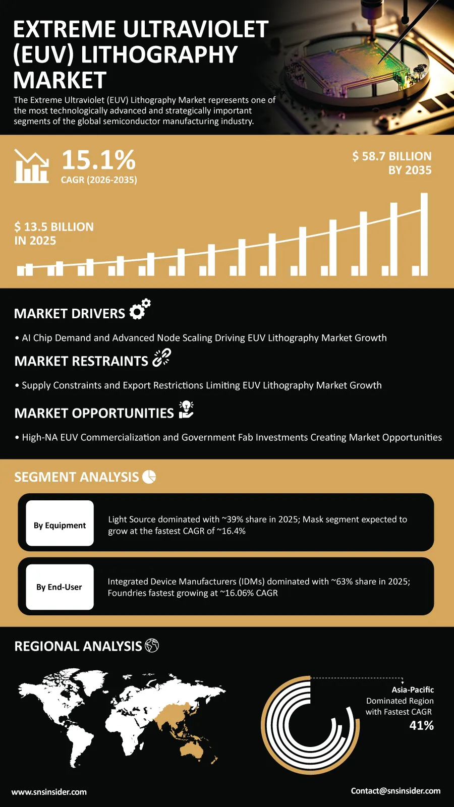
The global Extreme Ultraviolet (EUV) Lithography Market is entering a transformative phase as semiconductor manufacturers accelerate investments in advanced process technologies to meet rising demand for artificial intelligence, high-performance computing, advanced smartphones, and next-generation memory. According to a recent study by SNS Insider, the global Extreme Ultraviolet (EUV) Lithography Market size valued at USD 13.5 billion in 2025, is anticipated to grow to USD 58.7 billion by 2035, registering a CAGR of 15.1% over the 2026–2035 forecast period.
The move toward 3nm, 2nm, and beyond node technologies is underpinning the growing strategic significance of EUV tools in wafer fabrication. The growing need for semiconductor manufacturers to benefit from the latest advances in lithography in order to produce ever smaller and more complicated circuit structures is driving up the demand.
Growing demands are also fueled by the growth in semiconductor wafer fabrication capacity worldwide. Strategic investments designed to boost domestic chip production capacity in North America, Europe, and Asia are generating further demand for EUV tools and associated equipment.
To Get Detailed Insights on the Extreme Ultraviolet (EUV) Lithography Market – Request a Sample Report
Advanced Semiconductor Manufacturing Creates New Growth Opportunities
The fast growth of AI infrastructure has created a high demand for powerful processors and accelerators that can be produced using state-of-the-art process technologies. In pursuit of higher computer performance in smaller designs, semiconductor manufacturers are investing more in lithography machines.
High-NA EUV technology has become an important market opportunity due to the resolution enhancement for the next sub-2nm process technology nodes. At the same time, advancements in the field of photoresist, photomask, pellicle, and inspection technologies are addressing the technological issues related to the high-volume EUV production.
The diversification of the geographic locations of semiconductor manufacturing is another important market opportunity. The new fabrication facilities supported by government funding are likely to contribute to the growth of the EUV systems market demand.
Key Market Insights Highlight Shifting Demand Patterns
By equipment, the light source segment is expected to account for approximately 39% of global market revenue in 2025, reflecting its critical role in generating the 13.5nm radiation required for EUV exposure. The mask segment is projected to be the fastest-growing equipment category, advancing at a CAGR of approximately 16.4% through 2035 as chipmakers address increasingly demanding patterning requirements at advanced nodes.
Based on end user, integrated device manufacturers (IDMs) are anticipated to hold approximately 63% of market revenue in 2025, supported by major investments from companies operating integrated design and manufacturing facilities. Foundries are expected to register the fastest growth, with a CAGR of approximately 16.06%, as the expansion of fabless chip design and outsourced semiconductor production drives demand for advanced manufacturing capacity.
AI and Process-Node Scaling Remain Key Market Catalysts
The global semiconductor industry is witnessing drastic structural changes as increased demand for advanced processing power driven by AI creates pressure on data centers, clouds, self-driving machines, and edge computing facilities. These use cases demand semiconductors combining powerful processing abilities and improved energy efficiency, making advanced manufacturing technologies all the more important.
Meanwhile, mobile chips, automotive computers, and high-end memory devices are adopting increasingly complex design. This creates an impetus for increasing EUV capacity and investing in process technologies capable of raising wafer output and improving yields.
Although, the expense and complexity associated with EUV technologies pose significant challenges. Constraints on manufacturing capacity, equipment delivery times, component specifications, and geopolitical limitations on technology trade continue to define market dynamics.
Asia Pacific Leads with 41% Revenue Share While North America Advances at a 16.3% CAGR
The Asia Pacific region will continue to dominate the market, capturing around 41% of the total global revenue in 2025. In terms of advanced semiconductors manufacturing centers, the Asia Pacific region accounts for Taiwan and South Korea, thanks to the investments made by key foundry and memory makers.
North America is forecast to be the fastest-growing region with an anticipated CAGR of around 16.3% through 2035. Advanced-node production capability in North America is being driven by various incentives for semiconductor chips in the U.S. and the initiation of new fabs.
Europe plays a strategically significant role in the industry owing to the presence of EUV technology development and semiconductor equipment capabilities. In the meantime, developing markets in the Middle East, Africa, and Latin America still account for the early phase of implementation of EUV technology owing to the high infrastructure and capital needs.
Industry Participants Focus on High-NA Innovation and Advanced Manufacturing
The competitive landscape is highly specialized, with industry participants concentrating on increasing EUV source power, improving optical precision, advancing mask technologies, and developing solutions that enhance production yields. The emergence of High-NA EUV is expected to intensify technology competition as semiconductor manufacturers prepare for future process generations.
Key companies operating in the global Extreme Ultraviolet (EUV) Lithography Market include ASML Holding NV, Taiwan Semiconductor Manufacturing Company (TSMC), Samsung Electronics Co., Ltd., Intel Corporation, SK Hynix Inc., Micron Technology Inc., ZEISS Group, Toppan Photomasks Inc., Dai Nippon Printing Co., Ltd. (DNP), Photronics Inc., AGC Inc., Ushio Inc., Gigaphoton Inc., Synopsys Inc., Cadence Design Systems Inc., Applied Materials Inc., Tokyo Electron Ltd., KLA Corporation, Lam Research Corporation, and Entegris Inc.
An SNS Insider analyst Sushant Kadam commented, “The accelerating demand for AI computing, advanced processors, and next-generation semiconductor technologies is strengthening the strategic importance of EUV lithography. As chipmakers expand leading-edge capacity and transition toward sub-2nm manufacturing, advancements in High-NA systems, mask technology, and process control will create substantial opportunities across the EUV ecosystem.
About the Author

Get in touch