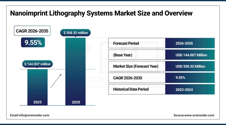
As per the SNS Insider Report titled, Nanoimprint Lithography Systems Market by Type, by Application, by End-User, by Technology, and Region | Global Forecast 2026-2035, “The global Nanoimprint Lithography (NIL) Systems Market size valued at USD 144.007 million in 2025, is anticipated to grow to USD 358.32 million by 2035, registering a CAGR of 9.55% over the 2026–2035 forecast period.”
Key Takeaways
-
UV-based Nanoimprint Lithography (UV-NIL) accounted for nearly 63.80% of the market share in 2025, driven by its high-resolution patterning capabilities and increasing adoption in semiconductor fabrication processes.
-
Hot Embossing (HE) is projected to witness the fastest growth during 2026–2035 due to rising demand for cost-effective and high-throughput nanofabrication technologies.
-
Semiconductors dominated the application segment with a 46.30% revenue share in 2025 owing to increasing demand for advanced chip manufacturing and nanoscale patterning technologies.
-
Semiconductors are also expected to register the fastest growth through 2035 supported by rising investments in advanced semiconductor node development and next-generation electronic devices.
-
Semiconductor Foundries held approximately 42.60% share in 2025, supported by growing integration of nanoimprint lithography systems into advanced semiconductor manufacturing workflows.
-
Semiconductor Foundries are anticipated to emerge as the fastest-growing end-user segment during the forecast period due to increasing demand for high-precision nanoscale fabrication solutions.
-
UV-based Nanoimprint Lithography dominated the technology segment with a 51.80% market share in 2025 owing to its efficiency, scalability, and compatibility with high-volume manufacturing applications.
-
UV-based Nanoimprint Lithography is projected to maintain the strongest growth trajectory through 2035 driven by increasing applications across semiconductors, photonics, and advanced electronics manufacturing.
-
Asia-Pacific captured around 39.40% of total market revenue in 2025 and is expected to strengthen its market position further through 2035 supported by expanding semiconductor fabrication infrastructure and electronics manufacturing activities.
-
North America accounted for approximately 28.60% of the global market share in 2025 driven by strong investments in semiconductor research, nanotechnology innovation, and advanced manufacturing capabilities.
Why Nanoimprint Lithography Systems Market is Growing?
The Nanoimprint Lithography Systems Market has been growing steadily due to growing needs for advanced nanotechnology solutions in various industries such as semiconductor manufacturing, photonics, biotechnology, and electronics. Nanoimprint lithography is known to provide higher resolution pattern formation processes than traditional lithography technologies while incurring relatively low production costs.
The increase in capital investments in advanced semiconductor nodes and small-scale electronic device development has fueled the growth of this market to a great extent. The semiconductor companies have increasingly been turning towards the use of nanoimprint lithography systems to help fabricate advanced integrated circuits and other advanced computing applications.
Moreover, the increasing implementation of nanotechnology-based solutions in various industries including optics, biomedical research and applications, and flexible electronics, among others, has boosted demand for nanoimprint lithography solutions. The rise in the use of UV-based nanoimprint technologies has also boosted demand in the global market.
Furthermore, advances made in the area of mold formation and precise alignment systems, amongst others, are expected to drive the market.
Nanoimprint Lithography Systems Market Statistics
-
The semiconductor industry is making significant investments in the development of nanoimprint lithography solutions for advanced nanolithography processes in chip fabrication.
-
The popularity of UV nanoimprint lithography systems will grow further as a result of their suitability for large-scale semiconductor production processes.
-
The increasing demand for miniaturized electronic products and semiconductor nodes is driving the use of advanced nanolithography technologies.
-
Nanoimprint lithography is becoming increasingly used in semiconductor foundries for advanced packaging and photonic devices manufacturing.
-
Nanoimprint lithography technology finds new areas of application in biotechnology, optics, flexible electronics, among other nanotechnology domains.
-
As far as regions, Asia-Pacific will retain its position as the dominant player, with growing semiconductor manufacturing capacity.
-
Scientific organizations and advanced manufacturing centers are increasing investments in nanofabrication techniques.
Emerging Trends
Transformative trends observed within the Nanoimprint Lithography Systems Market include the adoption of high-speed UV nanoimprint technology for use in the manufacturing of semiconductors and photonics applications. Manufacturers are concentrating on the enhancement of nanoscale accuracy, scalable processes, and efficient production to enable advanced electronic device production.
Newly developed semiconductor packaging technologies and heterogeneous integration technology are being seen as key growth opportunities due to the growing need for compact and powerful chip architecture. Hot embossing technology is also witnessing increased popularity for its role in the economic replication of nanostructures and flexible electronics manufacturing.
The market is also experiencing increased incorporation of automation, AI-enabled manufacturing processes, and precision alignment equipment in the manufacturing of nanoimprints. Finally, continued advancements in semiconductor foundries and nanotechnology research as well as photonic devices are likely to drive growth in the market going forward.
Top 10 Companies
-
Canon Inc.
-
EV Group (EVG)
-
Obducat AB
-
Nanonex Corporation
-
SUSS MicroTec SE
-
NIL Technology ApS
-
Toshiba Corporation
-
Molecular Imprints Inc.
-
AMO GmbH
-
STMicroelectronics
About the Author

Get in touch
